Sergey Pereverzev (13-ERD-016)
Abstract
Decreasing the noise and increasing the sensitivity of superconducting devices and increasing the coherence time of superconducting quantum bits (qubits) are important technical and scientific goals for developing new quantum sensors for national security applications and for superconducting quantum computing. Low-temperature noise in superconducting devices is caused by two-level systems (or fluctuators), objects that are capable of changing state at low temperatures. A common example of such a system is an atom that can tunnel between two adjacent equilibrium positions in the lattice arrangement of particles for a compound or in disordered glass. Additional sources of noise inside superconductors include magnetic moments (spins), magnetic ordering that can coexist with superconductivity at low temperatures, and glass-type behavior, among others. Current theoretical understanding of the effects of fluctuators on superconducting device noise and decoherence has not been sufficiently developed. For this project, we developed experimental approaches to reveal and understand fundamental noise mechanisms at radio-frequencies in superconducting devices in high-electric fields at ultralow temperatures. We explored the possibility of fabricating resonators and superconducting quantum interference devices (SQUIDs) out of single crystals composed of isotopically pure, zero-nuclear-spin materials to avoid nuclear spins in materials and localized electron spins on inter-grain boundaries in metal. The results of our work will guide development of new materials and new production technologies for quantum sensors and quantum computers.
Background and Research Objectives
Two-level system fluctuators in solid-state electronic or superconducting devices can change their state because of thermal or quantum fluctuations or by interactions with a superconducting device. Alternately, state changes can be driven while reading the device and by electromagnetic noise, which is not yet detectable by other means and can leak into the experiment from the environment. The short coherence times obtained in state-of-the art devices can be explained by the presence of a small number of two-level systems in the materials making up the device. Superconducting microwave resonators are relatively easy to fabricate and have noise characteristics that are sensitive to the presence of two-level systems. Thus, one needs only to look at the performance of the resonator, and use it as a measure of the presence of two-level systems, seen in the resonance frequency jitter at the parts-per-million level at low temperatures. For niobium resonators and for the molybdenum–rhenium alloy, frequency jitter at low temperatures increases with cooling, a phenomenon that is still difficult to explain. This behavior was observed for polycrystalline niobium film on silicon1 and for epitaxial niobium on sapphire, as well.2 In SQUIDs, small fluctuations of magnetic flux through the SQUID loop can be observed.3 Changes in the inductance of the SQUID loop correlate with flux fluctuations,4 for which there is not yet a good explanation.
Many attempts have been made to improve performance of these devices, typically by introducing a small variation in production technologies.5 A number of groups are examining new superconducting materials, but are keeping the same production techniques or the same substrate materials, which are potentially noisy. With this project, we aimed to construct a different, more radical experimental approach.
Two-level systems are believed to be present in dielectrics or at dielectric–metal interfaces. We note that dielectric substrates can be avoided or, at least, the noise-critical elements can be suspended. Thus, to study two-level systems in superconductors, we designed, modeled, and built prototypes of thin-metal-plate, slot-line resonators where one or several types of fluctuators could be removed. In addition, we investigated another device, the parallel-plate resonator, which has a gap that is thinner than its wavelength.6 We also determined a number of magnetometer experiments that could detect the presence of localized electron spins on surfaces.
Scientific Approach and Accomplishments
We started removing different classes of two-level systems by removing the dielectric substrate. Common superconducting materials like niobium or aluminum always have oxide film on a metal surface, but we can choose superconducting materials resistant to oxidation. In traditional methods, many impurities can enter the metal on inter-grain boundaries, but this can be avoided if devices are made out of single-crystal metal. By making a slot-line resonator out of a thin, single-crystal plate of metal that is stable to oxidation, we should be able to eliminate two-level systems of the most known type: atoms or ions having two closely spaced equilibrium positions near defects or near the surface. We eliminated them on substrate–metal interfaces, on inter-grain boundaries, and in dielectric substrate by removing the dielectric substrate itself. It is still possible to have lattice defects in the bulk single crystal, though in much smaller concentrations, or in small interstitial atoms such as hydrogen that are capable of tunneling between two or more locations in a bulk single-crystal’s lattice.7
It is often assumed that at metal–dielectric interfaces, a number of localized electrons are capable of changing the orientation of their magnetic moment, affecting their spin or their orbit. This causes residual fluctuation of magnetic flux through the SQUID loop.3 The number of those magnetic moments should be significantly reduced when no substrates and no oxide layer are present. The existence of those localized surface electron states has been confirmed by independent experiments. We expected that the magnetometer measurements of a stack of 100 to 500 thin foils could confirm their existence, and performed an initial test of thin sapphire samples, and planned to continue this with both sapphire and thin metal foils.
Magnetic impurities inside superconductors also create problems with the nuclear magnetic moments of the superconductor’s constituent material. Nuclear magnetic moments are approximately 1,000 times smaller than the magnetic moments of an electron, and they are usually ignored for this reason. The effect of independent fluctuations of nuclear magnetic moments is indeed smaller than that of electron or ion spins.8 On the other hand, magnetic moments in metal can interact with each other through conductivity electrons, known as RKKY (Ruderman–Kittel–Kasuya–Yosida) interactions, which can lead to magnetic ordering and can co-exist with superconductivity.9 The appearance of clusters of nuclear ordering should lead to a change of electrochemical potential for electrons inside a cluster, and could result in correlated fluctuations of the magnetization, kinetic inductance, and charge of the cluster.
Using high-purity isotopes with zero nuclear spins significantly reduce the number of magnetic nuclei inside a superconductor. Zero-spin nuclei also have no nuclear quadrupole electric moments, which interact with the local electric-field gradient. So even in the absence of a magnetic field, the energy of the nuclei inside the lattice depends on their orientation. This results in nuclear quadrupole resonance, or zero-field nuclear magnetic resonance, which is in the megahertz frequency range for many materials. For the sites around lattice defects, the local electric field and local electric-field gradient could be strongly enhanced (the giant flexo-electric effect). For example, hetero-epitaxial boundaries are prone to forming lattice defects to compensate for small lattice-parameter mismatches.10 As a result, quadrupole resonance frequencies for defect sites could be shifted to gigahertz range and could interfere with qubit operation. Additionally, the existing theoretical models of nuclear magnetic ordering are not complete—they do not take into account quadrupole interactions of nuclei with local electric-field gradients and, through lattice deformations, with each other. This makes direct experimental investigation even more important.
In the absence of reliable theoretical models, experiments need to be performed in a consistent and conservative manner, without introducing too many changes simultaneously, which pose restrictions on the materials we could use for tests. We could not check the effects of nuclear spins with niobium or aluminum (which are in wide use for SQUIDS and qubits) because there are no stable isotopes of these elements with zero nuclear spin. In addition, it is almost impossible to avoid surface oxide layers on aluminum or niobium devices. It is relatively easy to produce single crystals on lead, tin, or zinc, because those metals have relatively large superconducting transition temperatures (superconductivity is the total disappearance of electrical resistance below a definite temperature called the transition temperature), and zero-spin and non-zero-spin isotopes are readily available. Preserving oxide-free and, therefore, patina-free single-crystal metal surfaces in low-temperature experiments was demonstrated for zinc, but was not simple. Producing the slot-line resonator and preserving oxide-free metal surfaces within it was also found to be difficult. Molybdenum and tungsten will not oxidize on contact with air, and their zero-spin isotopes are commercially available. Molybdenum single crystals are commercially available and relatively easy to grow using melting zone recrystallization, which also can be used to purify the material. Tungsten has two crystallographic modifications, and at present there is no reliable technology to grow large single crystals. One phase of tungsten has a transition temperatures above 4 K, so we believe it would be scientifically interesting to pursue technology for developing this phase.
Accordingly, we decided to start with a molybdenum slot-line resonator. The pattern of slots needed to be singly connected and self-supported. The range of resonance frequencies that we can measure at present is limited by our equipment to 4 to 8 GHz. A smaller-sized resonator is preferable because single-crystal isotope samples are costly, and growing large single crystals is more difficult. We found that multiple split-ring resonator geometry11 provides a reasonable compromise between small size, sufficiently low frequency, and mechanical stability. Another technical requirement was to provide proper coupling of the resonator and transmission line used for measurements. The usual practice is to make multiple resonators with different coupling to the transmission line, which is formed on the same chip. We decided to produce the transmission line in the form of a wire parallel to the surface of a metal plate. Changing the distance between the transmission line and the resonator provides adjustment of coupling. According to our modeling results, a motion range of a few millimeters is sufficient, which made it easy to provide for our 5- to 8-mm resonators. This resonator size was larger than that of resonators made on a substrate because the dielectric constant of our dielectric vacuum was smaller than that of our dielectric substrate (usually 6 to 8 mm).
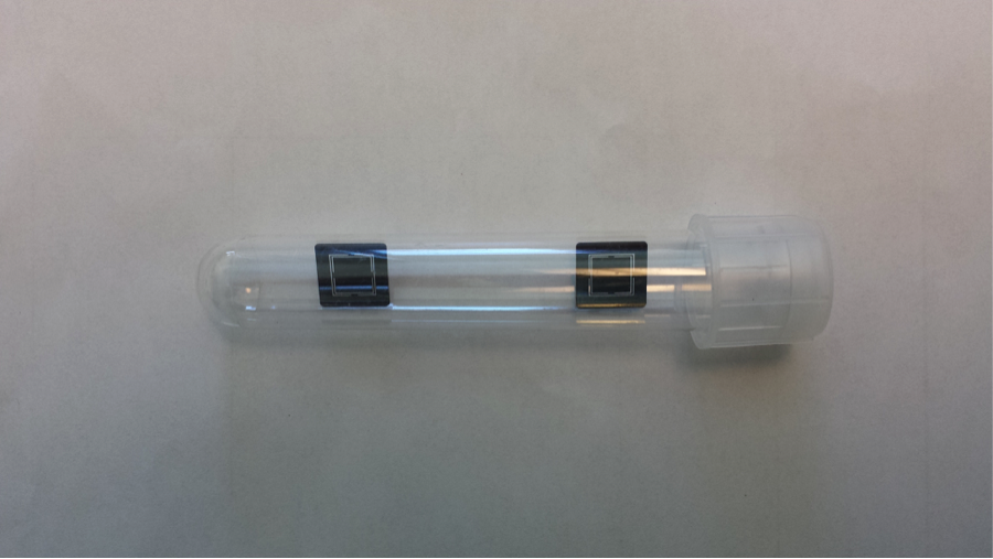
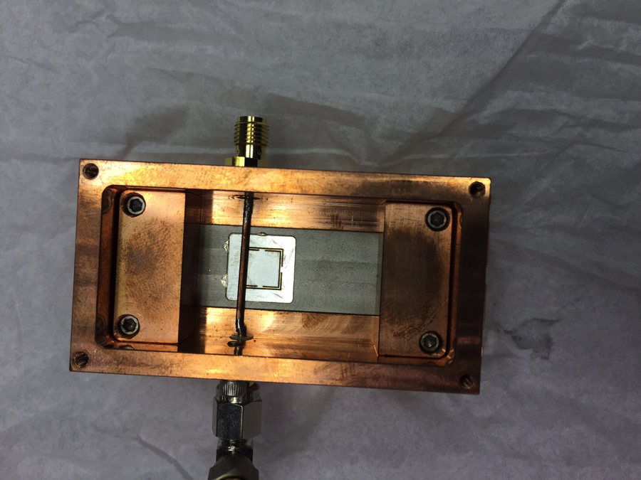
We produced our first sample resonators out of a 100-mm-thick molybdenum plate by making 200-mm cuts using in-house LLNL laser-cutting methods (Figure 1). We also designed and made our first prototype resonator box out of copper with a 2-mm-thick resonator support plate made out of molybdenum—this plate minimized mechanical stress caused by thermal contraction (Figure 2). Before we moved to single-crystal samples, we practiced electrochemical polishing and etching of samples after laser cutting.
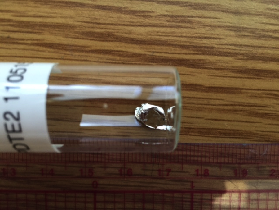
Some superconducting alloys are stable to oxidation and their component elements all have zero-spin isotopes. Those alloys—palladium–silicon, platinum–silicon, and palladium–thallium—were used for making superconducting devices, but we do not have a reliable technology to grow single crystals out of those materials. Palladium–tellurium has a transition temperatureabove 4 K,12 but grooving large, single crystals could be difficult because the recrystallization of palladium–tellurium should take place while cooling from melt. Palladium–tellurium single-crystal growth is possible during melt with stoichiometric composition, and it has a transition temperature above 1 K. Work on synthesizing palladium–tellurium single crystals is ongoing (Figure 3). These samples are especially interesting to obtain because palladium–tellurium is a superconductor whose topological surface states coexist with superconductivity when in bulk.13
Impact on Mission
By increasing scientific understanding of how to decrease noise and increase sensitivity of superconducting devices, the research conducted in this project will lead to quantum sensors for national security applications in chemical and radiation detection, as well as for superconducting quantum computing. This work supports the Laboratory’s central missions in national security and reduction of nuclear threats, as well as the strategic focus area in cyber security, space, and intelligence.
Conclusion
Through our research, we are now in a unique position to determine the roles of several classes of two-level system (fluctuators) on noise and decoherence in superconducting devices in controlled experiments. We have learned how to model the operation of several types of superconducting microwave resonators that can be used for materials research. This modeling work should be expanded to other devices, including SQUIDS. We have started work on synthesizing new superconducting single-crystal materials, including topological superconductors, which eliminate two-level systems associated with atoms jumping on near-defect sites. We envision low-temperature magnetometry as a method to study electron spins on surfaces and interfaces as well as their dependence on surface passivation and a high electric field on the surface to minimize the number of surface electron spins and their effect on noise at low temperatures. Development of SQUIDs out of new material could have a strong impact on the field by making possible more sensitive measurements.
Two LLNL records of invention resulted from this work: "Isotopically Pure Materials for Ultra-Low Noise Cryogenic Devices and Q-bits" and "High-Voltage Distribution System for Cryogenic and Vacuum Applications.” Based on these, we have applied for a patent for our “Single-Crystal Zero-Nuclear-Spin Materials and Devices for Quantum Computing and Ultra-Low-Noise Cryogenic Devices.” The idea allows a significant reduction in noise and decoherence, and corresponding micro-fabrication technologies could be developed and used to improve SQUIDs, photon detectors, microcalorimeters, superconducting mixers, and other detectors. Those materials and technologies also can be used to create more efficient superconducting computers and to increase coherence time of superconducting qubits, thus providing a path for superconducting quantum computing.
References
- Kumar, S., et al., “Temperature dependence of the frequency and noise in superconducting coplanar waveguide resonators.” Appl. Phys. Lett. 92, 123508 (2008). http://dx.doi.org/10.1063/1.2894584
- Burnett, J., et al., “Evidence for interacting two-level systems from the 1/f noise of a superconducting resonator.” Nature Comm. 5, 4119 (2014). http://www.nature.com/ncomms/2014/140617/ncomms5119/full/ncomms5119.html
- Choi, S., et al., “Localization of metal-Induced gap states at the metal–insulator interface: Origin of flux noise in SQUIDs and superconducting Q-bits.” Phys. Rev. Lett. 103, 19701(4) (2009). http://journals.aps.org/prl/abstract/10.1103/PhysRevLett.103.197001
- Sendelbach, S., et al., “Complex inductance, excess noise, and surface magnetism in DC SQUIDs.” Phys. Rev. Lett. 103, 117001(4) (2009). http://journals.aps.org/prl/abstract/10.1103/PhysRevLett.103.117001
- Martinez, J. M., and A. Megrant, “UCSB final Report for the CSQ program: Review of decoherence and materials physics for superconducting qubits.” Quant. Phys. 1410.5793 (2014). http://arxiv.org/abs/1410.5793
- Taber, R. C., “A parallel plate resonator for microwave loss measurements on superconductors.” Rev. Sci. Instrum. 61, 2200 (1990). http://dx.doi.org/10.1063/1.1141389
- Philips, W. A., “Two-level states in glasses.” Rep. Prog. Phys. 50, 1657 (1987).
- Laforest, S., and R. de Sousa, “Flux-vector model of noise in superconducting circuits: Electron versus nuclear spins and role of phase transition.” Phys. Rev. B 92, 054502 (2015). http://journals.aps.org/prb/abstract/10.1103/PhysRevB.92.054502
- Rehmann, S., et al., “Interplay of nuclear magnetism and superconductivity in AlIn2.” Phys. Rev. Lett. 78, 1122 (1997).
- Lee, D., and T. W. Noh, “Giant flexoelectric effect through interfacial strain relaxation.” Phil. Trans. Roy. Soc. Lord. Math. Phys. Sci. 370, 4944 (2012). http://rsta.royalsocietypublishing.org/content/roypta/370/1977/4944.full.pdf
- Bilotti, F., et al., “Design of spiral and multiple split-ring resonator for the realization of miniaturized metamaterial samples.” IEEE Trans. Antenn. Propag. 55, 2258 (2007). http://ieeexplore.ieee.org/stamp/stamp.jsp?arnumber=4285968
- Mattias, B. T., “Transition temperatures of superconductors” Phys. Rev. 92, 874 (1953). http://journals.aps.org/pr/abstract/10.1103/PhysRev.92.874
- Liu, Y., et al., “Identification of topological surface state in PdTe2 superconductor by angle-resolved photoemission spectroscopy.” Chinese Phys. Lett. 32(6) (2015). http://iopscience.iop.org/article/10.1088/0256-307X/32/6/067303?fromSearchPage=true1


