Selim Elhadj (15-ERD-057)
Abstract
Transparent conductive electrodes fulfill essential functions in optical-electronics applications including light-harvesting solar cells, display panel controls, and energy-efficient windows with selective light filtering. Compact high-repetition-rate lasers use Pockels cells that also require transparent conductive electrodes. In addition, these electrodes are found in spatial light filters such as those used for damage management in high-fluence lasers and in systems being explored for rapid additive manufacturing. In these demanding applications, transparent conductive electrodes are often limited by optical damage. We plan to develop processes, along with materials used in the electrodes, that can withstand irradiation from high-power lasers. Optoelectronics film susceptibility to optical damage can limit laser power and add steep design constraints to a laser and its size. We will determine optical failure modes and produce high-damage-threshold transparent conductive electrodes with fast electrical transport. This will be achieved by probing next-generation wide-gap semiconductors prepared using conventional and new thin-film fabrication techniques coupled to enhanced laser annealing.
We expect to identify optical failure modes and optimized fabrication of transparent conductive electrodes on robust substrates using conventional and new film synthesis approaches that include enhanced laser annealing. We will assess films with respect to the optical damage threshold and conductivity trade-off. This knowledge and capability can support development of high-power lasers—for example, repetition-rated, high-average-power and small form-factor lasers being deployed in scientific exploration. Computational capability will be established that simulates laser sintering of nanometer-scale particles that minimize film defects and can impact additive manufacturing. In addition, we will develop the capability for doped nanometer-scale particle-synthesis building blocks.
Mission Relevance
This work can enable and enhance performance of high-power lasers used in core missions throughout the Laboratory, including lasers for inertial fusion energy, and potentially new laser systems for parallel, fast laser-based additive manufacturing technologies in support of LLNL core competencies in lasers and optical science and technology and advanced materials and manufacturing. Extending our understanding of transparent conductive electrodes synthesis and optical failure modes may also support the strategic focus area in cyber security, space, and intelligence for protection of systems that rely on high-performance optoelectronics. Finally, transparent conductive electrode improvements can extend to multiple related applications involving energy production such as solar-cell transparent electrodes and conservation with selective light filters, relevant to the strategic focus in energy and climate security.
FY15 Accomplishments and Results
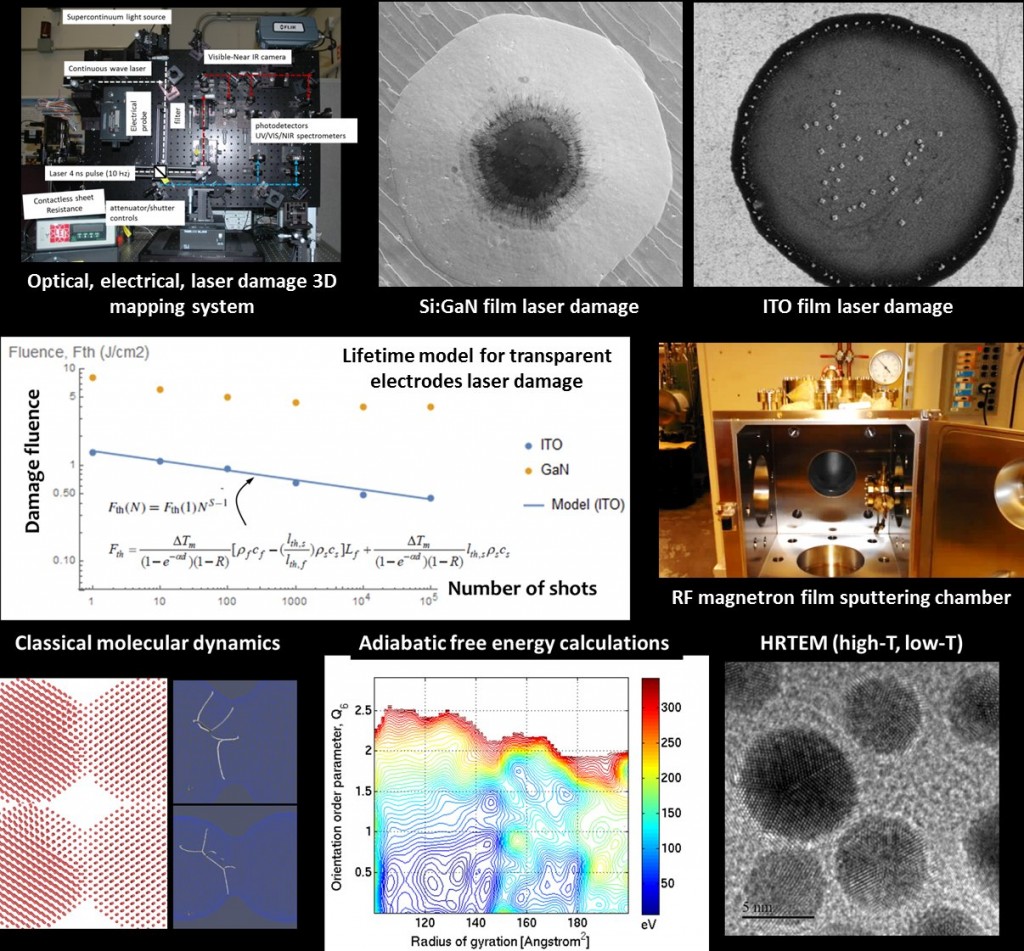
In FY15 we (1) determined laser output regimes for optical damage and lifetime performance of thin conductive films of indium tin oxide and doped zinc oxide exposed to near-infrared pulses; (2) determined that the films' damage performance degraded over repeated exposures; (3) developed a predictive model of degradation based on a material's optical and thermal properties and laser conditions; (4) identified three possible laser-output-dependent failure mechanisms involving photochemical, thermal and mechanical, and thermal processes; (5) demonstrated in-house hydrothermal growth of n-type doped zinc oxide (n-type refers to larger electron concentration than electron-hole concentration), and designed a film sputtering system; and (6) simulated heated grain-boundary dynamics with a novel atomistic scheme revealing boundary thickening.


