Ted Laurence (14-ERD-014)
Abstract
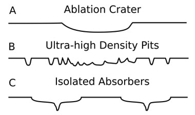
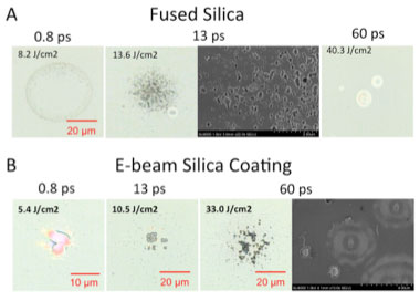
Laser-induced damage with picosecond pulse widths straddles the transition from intrinsic, multiphoton ionization- and avalanche ionization-based ablation with femtosecond pulses to defect-dominated, thermal-based damage with nanosecond pulses. We investigated the morphology and scaling of damage for commonly used silica and hafnia coatings, as well as fused silica. Using carefully calibrated laser-induced damage experiments, in situ imaging, and high-resolution optical microscopy, atomic force microscopy, and scanning electron microscopy, we showed that defects play an important role in laser-induced damage for pulse durations as short as 1 ps. Three damage morphologies were observed: standard material ablation, ultra-high-density pits, and isolated absorbers. For 10 ps and longer, the isolated absorbers limited the damage performance of the coating materials. We showed that damage resulting from the isolated absorbers grows dramatically with subsequent pulses for sufficient fluences. For hafnia coatings, we used electric field modeling and experiments to show that isolated absorbers near the surface were affected by the chemical environment (vacuum vs. air) for pulses as short as 10 ps. Coupled with the silica results, these results suggested that improvements in the performance in the 10–60 ps range have not reached fundamental limits. These findings motivated new efforts. A damage test facility for picosecond pulses was developed and automated, and was used for testing production optics for Livermore's Advanced Radiographic Capability. The resulting software was transferred to other laser test facilities for femtosecond pulses and multiple wavelengths with 30-ps pulses.
Background and Research Objectives
Laser-induced damage of optical materials is a particularly interesting example of a laser–material interaction in which the material itself is modified, often in ways contrary to its intended use. Laser-induced damage for sub-picosecond pulses and for pulses 1 ns and longer have been studied extensively. Thermal processes related to extrinsic absorption by materials not native to the host (bulk silica or air) dominate laser-induced damage in the nanosecond-scale regime.1 For short enough laser pulses (femtosecond regime) thermal processes no longer apply and multiphoton ionization and tunneling dominate. However, the physics governing the intermediate regime (1–100 ps) where typical pulse intensities range between 100 GW/cm2 and 1 TW/cm2 remained unclear. Models that explain the transition from defect-driven, thermal-based breakdown in the nanosecond regime, to photo-ionization- and avalanche ionization-induced free electron breakdown in the femtosecond regime are lacking, and measurements have not focused on this transitional pulse-width regime, with a few exceptions.2
Uncertainty in the physics driving the breakdown by pulses in the picosecond regime greatly complicates current efforts to model and improve performance limits and lifetimes of optics used in picosecond laser systems. For example, advanced short-pulse laser systems are typically limited in their final optics to < 0.5 TW/cm2 in the picosecond regime, making these systems inherently inefficient as well as large and costly. Additional studies focused on the mechanisms and materials involved in laser damage of picosecond-scale laser pulses are needed to help improve laser performance.
For short pulse lengths, multilayer dielectric coatings are used to create reflective optics that avoid nonlinear propagation issues through optical materials. Commonly used materials include silica and hafnia deposited in layers. By alternating layers of the low-index material (silica) and the high-index material (hafnia), it is possible to create highly reflective mirrors with greatly improved damage performance. The primary objective of this LDRD was to determine if the possibility exists to raise the fluence for the onset of damage.
The goals of the proposed scope were to (1) measure the short pulse (1–60 ps) damage precursor density and determine if intrinsic or extrinsic factors limit performance; (2) determine the effects of multiple short pulses, including growth and long-term degradation; (3) investigate the mechanisms of short-pulse laser damage and measure the key parameters for modeling; and (4) identify the dominant failure mechanisms and damage precursors and explore mitigation strategies.
Scientific Approach and Accomplishments
We accomplished these goals using an experimentally driven approach, coupling carefully calibrated laser-induced damage measurements with several high-resolution microscopic methods to understand the density and nature of the defects leading to damage. Several activities were critical to the interpretation of these results, including creating models for understanding damage scaling laws as a function of pulse width; extracting damage-precursor densities and optical field intensities in multilayer stacks; and investigating the propagation of fields through bulk silica and air.
A main goal of this project was to determine whether the laser-induced damage observed between 1 and 60 ps is due to intrinsic limitations or extrinsic factors such as defects. We studied the most common materials used to make multilayer reflective coatings in high-power laser systems: silica and hafnia. We performed measurements on silica and hafnia coatings as well as bulk fused-silica finished with the best surface finish. We used strategies developed for detecting defect densities in the defect-dominated nanosecond-pulse-length regime, including matching the position of damage to local fluences,3 as well as damage tests with varying beam sizes.4 For picosecond pulses on the entrance surfaces of optics, the damage site sizes tend to be much smaller (50 nm–5 μm) than corresponding damage on the exit surfaces with nanosecond laser pulses that are important for NIF-related studies. The small damage site size allows detection of defect-related densities much higher than found previously but requires the use of high-resolution microscopic methods to quantify the damage densities.
The laser-damage test experiments were performed at the laser-damage test facility in support of the Advanced Radiographic Capability (ARC) on the NIF. One beamline in vacuum was already in development for ARC-related damage testing.5–7 We developed a beamline in air that allowed for greater flexibility in adjusting beam size and allowing for higher fluence tests. It also allowed in situ imaging of the growth of laser-induced damage and a wider range of angle-of-incidence measurements. We developed software for controlling laser-damage testing, including correcting for beam energy and beam profiles, in situ monitoring of the damage process, and S/1 damage testing. (S/1 damage tests use a predetermined number of shots on a test site followed by a damage imaging and classification step.) We used the software in both beamlines and transferred it to other facilities.
We modeled the laser-induced damage process of ablation using standard models,2–8 and compared these results with extracted scaling laws. The difficulties and inconsistencies in fitting these experimentally determined scaling laws for 1–60 ps add support to the finding that defect-driven damage is dominant in this pulse-width range.
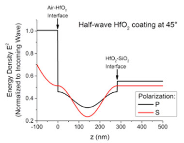
For hafnia coatings (Figures 3 and 4), we modeled the effects of the layers on the electric field distributions for varying input polarization and incident angles. This modeling effort allowed us to distinguish between the effects of surface defects and defects within the coating materials. We found that isolated absorbers on the surface of hafnia are affected by environmental conditions, with damage suppressed by the presence of air over vacuum (we do not know if oxygen or water suppressed the damage). That the chemical environment affects the progression of damage over a single 30-ps pulse indicates the complexity of the damage processes limiting the performance of these coatings.
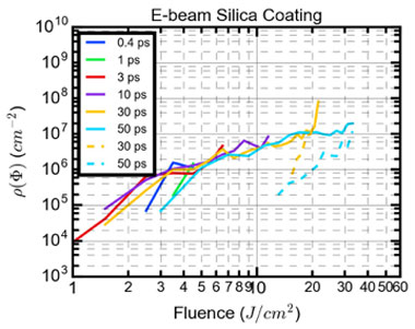
For the third goal of investigating damage mechanisms and measuring key parameters related to damage, we used multiple approaches. The high-resolution optical microscopy, atomic-force microscopy and scanning electron microscopy, helped us understand the nature of the absorber distribution. For measuring fundamental parameters, the initial focus was on measuring the key parameters of avalanche ionization-related ablation (avalanche ionization, multiphoton excitation coefficients, and relaxation times). The finding that defects were dominant in the development of laser-induced damage in this regime shifted the emphasis to finding the distribution of absorbers. A key finding was that initiation of the isolated absorbers was primarily dependent on fluence and much less dependent on pulse width (Figure 5). This indicates that the isolated absorbers are linear absorbers of energy. On the other hand, development of these isolated absorbers into growing sites is more dependent on pulse width (dotted lines in Figure 5). For short pulses less than 3 ps, the isolated absorbers have a limited effect on damage.
For the fourth goal of identifying dominant failure mechanisms and exploring mitigation strategies, we accomplished the first part through detecting the linear absorbers involved in laser damage of coatings. We performed unsuccessful annealing experiments; ramped R/1 tests indicated some possible marginal improvement with ramping the pulse energies. The need to reduce and eliminate the isolated absorbers indicated that a new method for depositing coatings need to be developed.
Impact on Mission
Optics for advanced, high-energy laser systems are required to withstand high peak power at pulse lengths from under 1 to 100 ps—some under high-repetition-rate, high-average-power conditions. By clarifying the fundamental mechanisms of laser–material interactions that cause laser-induced damage of optics coating materials under these extreme conditions, this project will lead to better design and operation of laser optics for high-power lasers. The project supports two of the Laboratory's core competencies: inertial-fusion science and technology and laser and optical science and technology, which contributes to the design of future high-energy and high-peak-power laser systems. The project also supports the Laboratory's strategic mission areas of stockpile stewardship, defense, and nonproliferation.
The project helped to convert one postdoctoral fellow to a full-time staff scientist position, increasing the Laboratory's depth of expertise in high-sensitivity microscopy applied to laser–material interactions. Also, this LDRD supported the retention and promotion of an important staff scientist in high-resolution dynamic microscopy and laser-damage testing. In addition to existing publications, three further publications are in preparation.
Conclusion
The discovery that defects in the coating materials dominate the laser-induced damage performance of these materials for pulses shorter than previously believed motivates continued work to improve the materials used in multilayer dielectric coatings. We observed that significant improvements in damage performance require changes in the deposition processes. An LDRD Strategic Initiative will build on this work by aiming to improve the deposition processes used for mirror production, focusing on the longer pulse regime from 30 ps to nanoseconds. Before this LDRD, it was well known that at short pulses, fundamental material processes lead to damage, and at long pulses, the processes are defect driven. We have shown that the defects play a role at shorter pulses than previously thought—defects must be considered even at pulse widths as low as 1 ps.
References
- Carr, C., J. Bude, and P. DeMange, "Laser-supported solid-state absorption fronts in silica." Phys. Rev. B 82, 184304 (2010).
- Stuart, B. C., et al., "Nanosecond-to-femtosecond laser-induced breakdown in dielectrics." Phys. Rev. B 53, 1749 (1996).
- Cross, D. A., and C. W. Carr, "Analysis of 1ω bulk laser damage in KDP." Appl. Opt. 50, D7 (2011).
- Laurence, T. A., et al., "Extracting the distribution of laser damage precursors on fused silica surfaces for 351 nm, 3 ns laser pulses at high fluences (20–150 J/cm2)." Optic. Express 20, 11561 (2012). https://doi.org/10.1364/OE.20.011561
- Alessi, D. A., et al., "Picosecond laser damage performance assessment of multilayer dielectric gratings in vacuum." Optic. Express 23(12), 15532 (2015). LLNL-JRNL-667566. https://doi.org/10.1364/OE.23.015532
- Negres, R. A., et al., "Apparatus and techniques for measuring laser damage resistance of large-area, multilayer dielectric mirrors for use with high energy, picosecond lasers." CLEO: Science and Innovations, Optical Society of America, SM3M.5 (2015). LLNL-ABS-665449. https://doi.org/10.1364/CLEO_SI.2015.SM3M.5
- Negres, R. A., et al., "Laser-induced damage of intrinsic and extrinsic defects by picosecond pulses on multilayer dielectric coatings for petawatt-class lasers." Optic. Eng. 56, 011008 (2016). LLNL-JRNL-690959. http://dx.doi.org/10.1117/1.OE.56.1.011008
- Mero, M., et al., "Scaling laws of femtosecond laser pulse induced breakdown in oxide films." Phys. Rev. B 71 (2005).
- Mero, M., et al., "On the damage behavior of dielectric films when illuminated with multiple femtosecond laser pulses." Optic. Eng. 44, 051107 (2005).
- Tzortzakis, S., et al., "Self-guided propagation of ultrashort IR laser pulses in fused silica." Phys. Rev. Lett. 87 (2001).
- Manes, K. R, et al., "Damage mechanisms avoided or managed for NIF large optics." Fusion Sci. Technol. 69, 146 (2016).
Publications and Presentations
- Alessi, D. A., et al., Picosecond laser damage assessment of multilayer dielectric diffraction gratings. (2016). LLNL-POST-679876.
- Negres, R. A., et al., "Characterization of laser-induced damage by picosecond pulses on multi-layer dielectric coatings for petawatt-class lasers." Proc. SPIE 9632, Laser-Induced Damage in Optical Materials. SPIE, Bellingham, WA (2015). LLNL-CONF-679191. http://dx.doi.org/10.1117/12.2195528
- Negres, R. A., et al., "Laser-induced damage of intrinsic and extrinsic defects by picosecond pulses on multi-layer dielectric coatings for petawatt-class lasers." Optic. Eng. 56(1), 011008 (2016). LLNL-JRNL-690959. http://dx.doi.org/10.1117/1.OE.56.1.011008


