Vincenzo Lordi (17-ERD-065)
Abstract
Semiconductor surfaces may represent a largely untapped resource for multifunctional heterogeneous catalysts. This is particularly true for resonant charge transfer reactions at solid/liquid interfaces, since the electronic structure of the surface can be tuned spatially and temporally. Well-controlled fabrication techniques may enable exquisite patterning of the surface to manipulate the electronic structure of interfaces and their consequent reactivity, which may be further controlled by external stimuli. The chemical potential of surface electrons dictates the rates of electrochemical charge transfer reactions and is dependent on the electronic charge and polarization of the interface, which are properties associated not only with the semiconductor’s band structure, but also modified by defects on the surface, and can be influenced by the molecular structure of liquid on the surface. This project uses first-principles atomistic simulations to investigate the impact of surface defects of missing atoms, or vacancies, on these properties for model semiconductor surfaces. Significant modification of both the molecular structure of interfacial liquid and the surface electrochemical potential is found near a vacancy, as opposed to the pristine surface. Differences in activity depending on the nature of the defect, such as its charge, are shown. These results motivate further studies to investigate the specific effects of a broader range of surface defects and interface atomic structures for these applications, as well as longer-range efforts to enable atomically precise fabrication techniques to control surface structure and composition at the atomic level.
Background and Research Objectives
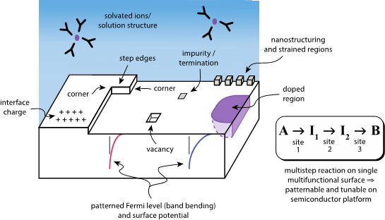
This project examines the feasibility of using atomically precise structures on the surface of a semiconductor to modify and control local electrocatalytic activity, in the context of creating novel multifunctional catalysts for multi-step chemical reactions. Specifically, we examined the effects of atomic-scale defects (i.e., “vacancies,” or missing atoms) that could be controllably produced to affect the spatial distribution of surface characteristics for catalysis. A range of atomic structures characterizes a complex semiconductor surface (see Figure 1); these structures may influence local catalytic activity both by modifying electronic structure and also by affecting the relative orientations of nearby molecules. We did not attempt to exhaustively examine all such structures, but rather focused on demonstrating the effects of model defects and compared a set of related but distinct materials. First-principles atomic-scale simulations were used to conduct the investigations.
This project focuses on heterogeneous charge-transfer reactions that are catalyzed by resonant alignment of energy levels at the catalyst/reactant interface, and thus provide an opportunity for a semiconductor surface to enable tunable multifunctionality. Many important driven reactions relevant to clean energy applications occur at semiconductor/liquid interfaces, such as photoelectrocatalytic fuel production from carbon dioxide (producing methanol), or from water (producing hydrogen). Traditional electrocatalysts tend to be comprised of metal surfaces, for which only limited and global tuning is possible via applied external bias potential to shift the surface Fermi level. The surface Fermi level is a key parameter for determining catalytic activity, since it relates to the alignment of catalyst energy levels with those of the reactants that drive the reaction (Lewis 2005; Hammer and Nørskov 1995 and 2001; Sabatier 1911; Balandin 1969). Semiconductor surfaces may be a largely untapped resource for heterogeneous catalysis, due to the possibility of spatio-temporal control of the local surface-electronic structure via manipulation of interface electronic charge, interface polarization, and surface band-bending through external or internal stimuli. In addition to stimuli such as light, applied voltage, doping, and solution composition, standard fabrication techniques (and future atomically precise fabrication techniques) may be used to pattern tunable multifunctionality on semiconductor surfaces.
The research goals of this project were to investigate the effects of surface vacancies on modifying electrocatalytic activity in model systems, in terms of (1) surface electrochemical potential and (2) the molecular structure of reactants. Three semiconductor materials were compared: gallium arsenide (GaAs), gallium phosphide (GaP), and indium phosphide (InP). Notable and significant changes in both the surface potential and the liquid structure in the vicinity of certain vacancy defects were found, motivating further detailed inquiry along this line of research.
Scientific Approach and Accomplishments
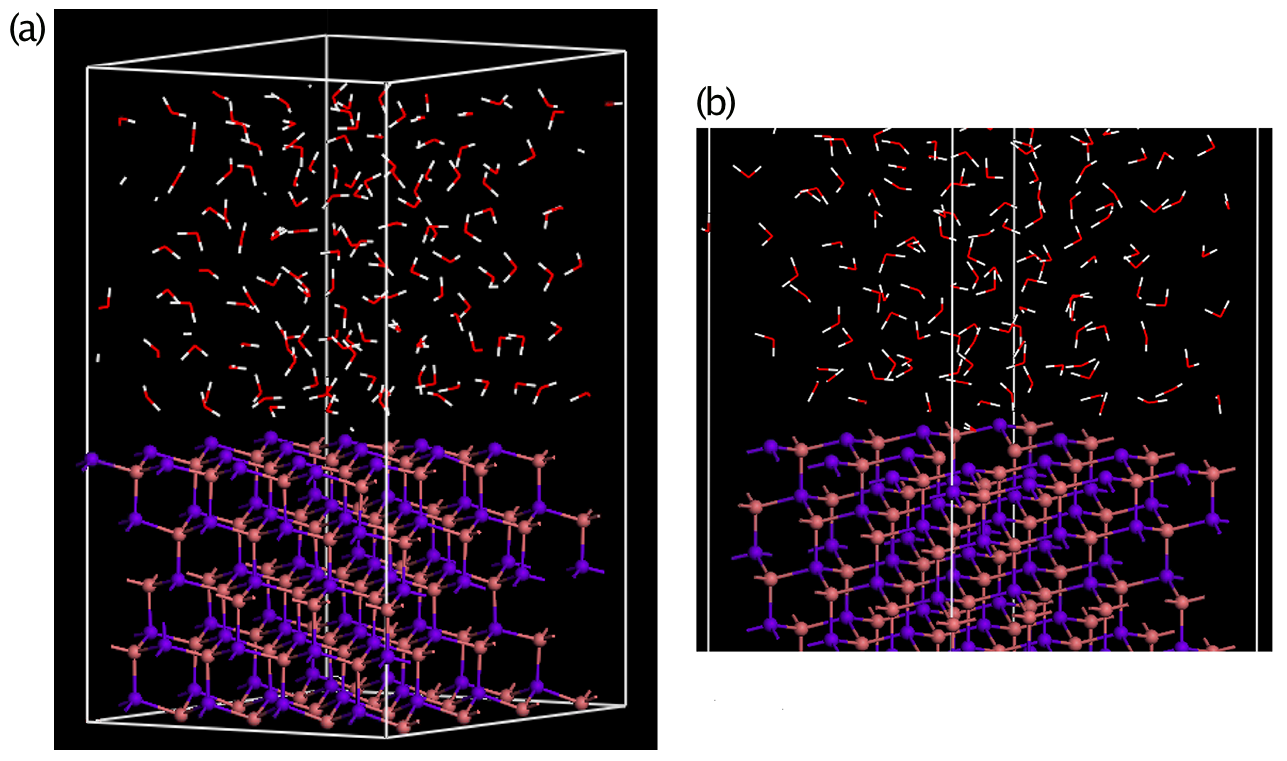
We used density-functional-theory-based simulations to explore the effects of defects on surface electron chemical potential of three model semiconductors (GaAs, GaP, and InP) in contact with liquid water. The structure and heterogeneity of real surfaces in electrochemical environments are very complex. We employed simplified model systems to focus on demonstrating the relevant effects without including all of the possible complexity. Specifically, we employed bare (111) oriented surfaces, as illustrated in Figure 2.
The pristine surfaces consist of close-packed planes of either cations (Ga, In) or anions (As, P) and are referred to as (111)A or (111)B surfaces, respectively. When allowed to relax, the flat surfaces reconstruct into a corrugated atomic configuration, with multiple reconstructions known for at least the (111)B surface (May et al. 2013); in this work, we only consider the most common of these configurations, the so-called (2x2). In addition, reaction with water can create complex and dynamic hydroxylated surface terminations, which also can lead to significant subsurface atomic rearrangements (Wood et al. 2011; 2013; and 2014); we did not consider hydroxylated surfaces specifically in this study. Nonetheless, the model systems used here generically demonstrate the mechanistic effect of local surface chemical potential shifts due to atomic-scale defects.
GaAs, InP, and GaP are good comparative semiconductors for this study, since they each catalyze the important fuel-generating CO2-reduction reaction, but require different amounts of applied overpotential to operate. They also have the same crystal structure and similar band structures, but have different absolute positions of their band edges and different band gaps (i.e., their intrinsic bulk electronic structures vary notably for catalytic purposes). The similarities facilitate construction of directly comparable simulation systems, while also providing a range of intrinsic surface chemical potentials for comparison.
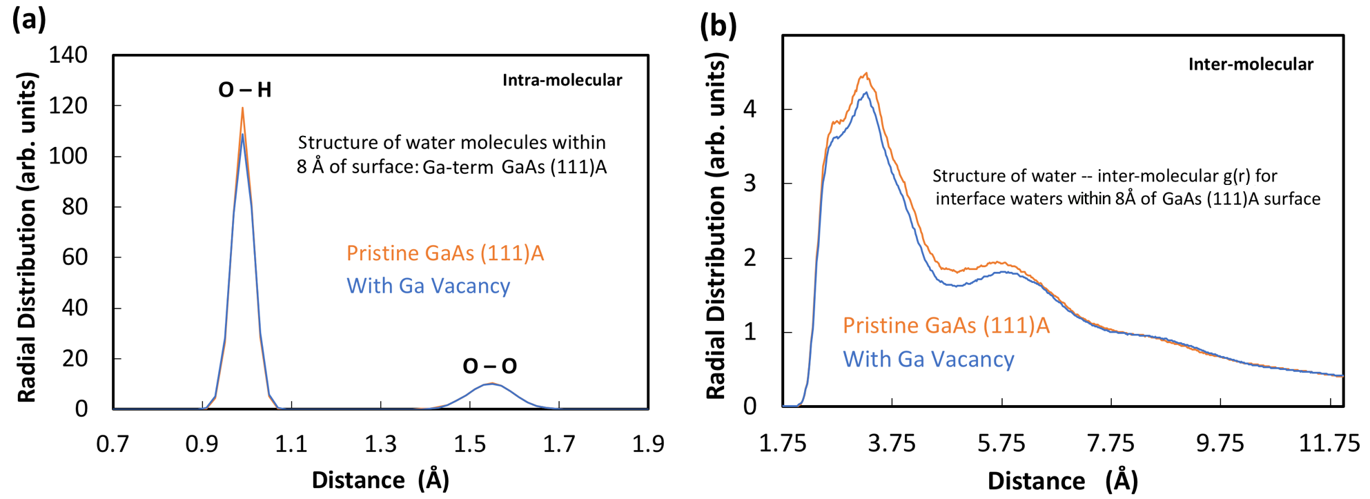
Local variation of reactivity associated with surface defects (e.g., step edges and vacancies) may be due to modification of either the solid surface electronic structure (i.e., chemical potential, or Fermi level) or the properties of the reactants in contact with the surface. We investigated changes in the structural properties (i.e., orientations, vibrations, and intermolecular bonding) of water molecules near the semiconductor surface when in the vicinity of a vacancy. In this context, water represents the solvent environment of a reaction system; modification of its intermolecular bonding network is indicative of altered reaction energy coordinate (for example, related to solvation energy or required molecular orientation) and consequent reactivity. Water may also comprise the reactant itself (for example, in a water-splitting reaction to produce hydrogen). We found that the presence of a surface vacancy slightly disrupted the intermolecular hydrogen bond network up to a few molecular layers away from the surface, with the effect being similar for the six investigated surfaces [(111)A and (111)B of GaAs, GaP, and InP]. Figure 3 shows representative results for the GaAs (111)A surface, presented in terms of the radial distribution functions of the atoms in water molecules within 0.8 nm of the surface. We observe a slight increase in intermolecular distances and a slight broadening of the oxygen–hydrogen (O–H) intramolecular-bond-distance peak in the presence of the vacancy, indicating weakening of the intermolecular-bond network. The surface vacancies were found to affect the local electrochemical potential.
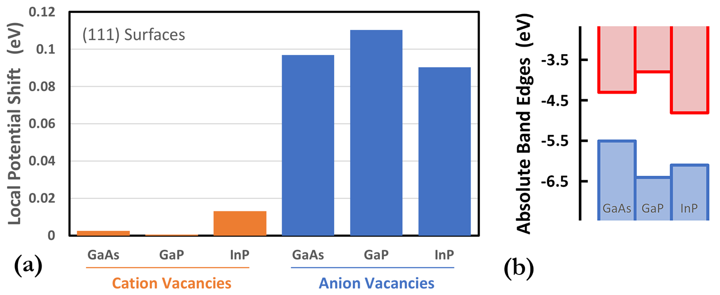
Figure 4(a) summarizes the computed changes in potential near a surface vacancy relative to the pristine surface for the six studied surfaces.
Note that the (111)A surfaces host cation vacancies, while the (111)B surfaces host anion vacancies. The potential shifts depicted in Figure 4(a) were computed by averaging the potential in a sphere centered at the vacancy position with a 0.35 nm radius. The results show a significant shift of approximately 0.1 eV for anion vacancies, but only a small effect for cation vacancies. More subtle differences were seen among the three materials. It is noteworthy that the sign of the shift is the same for both types of vacancies, despite their having opposite charge.
Surface potential is a critical parameter for driving reactions, since an alignment of energy levels between catalyst and reactant is generally required for charge transfer to occur. The shifts shown in Figure 4(a) are relative to the surface Fermi levels of each pristine material, which differ on an absolute energy scale. In particular, as shown in Figure 4(b), the valence band maximum of GaAs is 0.5–0.75 eV higher than that of GaP and InP, which are similar, while the band gap of GaP is considerably larger than that of both GaAs and InP (Stevanovic et al. 2014). Thus, choice of material sets the gross surface potential and catalytic activity, while fine local adjustment is possible by controlled placement of defects (vacancies). Given the range of absolute band edge positions, alloying (mixing) of the different compounds provides further gross control of the surface potential. Additional active control of the Fermi level within the band gap is achievable by doping or applying external bias voltage. The presence of surface defects enables fine tuning of the reactivity.
Details of Computational Methods
Simulations were performed using density functional theory within the projector augmented-wave method (Blöchl 1994; Kresse and Joubert 1999) as implemented in the VASP (Vienna Ab initio Simulation Package) code (Kresse and Furthmüller 1996a and 1996b). The generalized gradient approximation for the exchange-correlation potential in the PBE (Poisson–Boltzmann Equation) formulation (Perdew et al. 1996) was used. Wave functions were expanded in a plane-wave basis with energy cutoff of 350 eV. Slab models were constructed at least five stoichiometric layers thick to ensure recovery of bulk properties in the center of the slab, and 10–15 Å vacuum or water regions were included between periodic slab images. The in-plane dimensions of the slab supercells were either 3x3 or 4x4 unit cells. Brillouin zone sampling with 5x5x1 k-points was used for slab supercells. Slabs were constructed symmetrically, so that (111)A and (111)B facets terminated opposite sides of each slab; introduction of vacancies was also performed symmetrically, with cation and anion vacancies introduced together on the respective opposite faces. This symmetry ensured that supercells remained neutral to minimize otherwise spurious artifacts associated with charged supercells. Molecular dynamics simulations were performed using 0.5-fs time steps and a Nosé-Hoover thermostat (Nosé 1984; Hoover 1985) with period 0.62 ps.
Impact on Mission
This project is aligned with Lawrence Livermore National Laboratory's energy and climate security mission focus area, and supports its core competencies in high-performance computing, simulation, and data science, and advanced materials and manufacturing. Novel multifunctional catalysts can enable the production of clean, inexpensive chemical fuels in support of national energy security. Furthermore, the preliminary results from this project, in conjunction with related efforts at the Laboratory, provide leverage for helping to grow a portfolio in heterogeneous catalysis for energy applications, both through sponsor interactions and by helping build collaborations across other national laboratories and academic institutions in this field of research. This research also supports Livermore’s competency in high-performance computing for design of materials, specifically in the fields of materials for energy and heterogeneous catalysis.
Conclusion
This project investigated the possible effects of surface defects in enabling exquisite control of multifunctional catalytic surfaces based on semiconductors, using atomic-scale computer simulations. The results demonstrated the feasibility of this approach by showing significant modification of local reactivity due to potential shifts induced by vacancies on the surface of GaAs, GaP, and InP as representative atomic-scale structures. Further research is required to expand the work to a broader range of relevant materials, surfaces, and nanostructures for catalytic use, as well as investigate a broader suite of defects, including adatoms and atomic steps. Detailed simulations of specific electrocatalytic reaction mechanisms would be required to assess the quantitative impacts on a reaction of interest and help design a specific catalyst. To reliably create the designed surfaces at scale will require advances in specific fabrication technologies, such as atomically precise manufacturing and controlled hierarchical additive manufacturing.
References
Balandin, A. 1969. “Modern State of the Multiplet Theory of Heterogeneous Catalysis.” Advances in Catalysis 19: 1-210. doi: 10.1016/S0360-0564(08)60029-2.
Blöchl, P. E. 1994. “Projector Augmented-Wave Method.” Physical Review B 50:17953–17979. doi: 10.1103/PhysRevB.50.17953.
Hammer, B. and J. K. Nørskov. 1995. “Electronic Factors Determining the Reactivity of Metal Surfaces.” Surface Science 343 (3): 211–220. doi: 10.1016/0039-6028(96)80007-0.
——— 2001. “Theoretical Surface Science and Catalysis – Calculations and Concepts.” Advances in Catalysis 45: 71–129. doi: 10.1016/S0360-0564(02)45013-4.
Hoover, W. G. 1985. “Canonical Dynamics: Equilibrium Phase-Space Distributions.” Physical Review A 31: 1695–1697. doi: 10.1103/PhysRevA.31.1695.
Kresse, G. and J. Furthmüller. 1996a. “Efficient Iterative Schemes for Ab Initio Total-Energy Calculations Using a Plane-Wave Basis Set.” Physical Review B: Condensed Matter 54 (16): 11169–11186. doi: 10.1103/PhysRevB.54.11169.
——— 1996b. “Efficiency of Ab-Initio Total Energy Calculations for Metals and Semiconductors Using a Plane-Wave Basis Set.” Computational Materials Science 6 (1): 15–50. doi: 10.1016/0927-0256(96)00008-0.
Kresse, G. and D. Joubert. 1999. “From Ultra-Soft Pseudopotentials to the Projector Augmented-Wave Method.” Physical Review B 59 (3):1758–1775. doi: 10.1103/PhysRevB.59.1758.
Lewis, N. S. 2005. “Chemical Control of Charge Transfer and Recombination at Semiconductor Photoelectrode Surfaces.” Inorganic Chemistry 44 (20): 6900–6911. doi: 10.1021/ic051118p.
May, M. M., et al. 2013. “The Interface of GaP(100) and H2O Studied by Photoemission and Reflection Anisotropy Spectroscopy.” New Journal of Physics 15 (10): 103003. doi: 10.1088/1367-2630/15/10/103003.
Nosé, S. 1984. “A Unified Formulation of the Constant Temperature Molecular Dynamics Methods.” Journal of Chemical Physics 81: 511–519. doi: 10.1063/1.447334.
Perdew, J. P. et al. 1996. “Generalized Gradient Approximation Made Simple.” Physical Review Letters 77 (18): 3865–3868. doi: 10.1103/PhysRevLett.77.3865.
Sabatier, P. 1911. “Hydrogénations et Déshydrogénations par Catalyse.” Berichte der deutschen chemischen Gesellschaft 44: 1984–2001. doi: 10.1002/cber.19110440303.
Stevanovic, V., et al. 2014. “Assessing Capability of Semiconductors to Split Water Using Ionization Potentials and Electron Affinities Only.” Physical Chemistry Chemical Physics 16 (8): 3706–3714. doi: 10.1039/c3cp54589j.
Wood, B. C., et al. 2011. “Ab Initio Modeling of Water–Semiconductor Interfaces for Photocatalytic Water Splitting: Role of Surface Oxygen and Hydroxyl.” Journal of Photonics for Energy 1 (1): 016002–016011. doi: 10.1117/1.3625563.
——— 2013. “Hydrogen-Bond Dynamics of Water at the Interface with InP/ GaP(001) and the Implications for Photoelectrochemistry.” Journal of the American Chemical Society 135 (42): 15774–15783. doi: 10.1021/ja403850s.
——— 2014. “Surface Chemistry of GaP(001) and InP(001) in Contact with Water.” Journal of Physical Chemistry C 118 (2): 1062–1070. doi: 10.1021/jp4098843.


