Anna Hiszpanski (16-LW-041)
Project Description
Optical metamaterials (materials engineered to have properties not yet found in nature) are composites with periodic lattice structures that give rise to unique capabilities in guiding, confining, and propagating light. These metamaterials have generated significant interest for their potential uses as photonic crystals, which can serve as laser targets, and negative-index metamaterials, which have applications for super-lensing and invisibility cloaking. A negative-index metamaterial causes light to refract or bend differently from more-common positive-refractive-index materials. Optical metamaterials operate at visible wavelengths and are capable of being manufactured over large areas and are highly desirable for their diverse applications. However, challenges exist because such materials require lattice structures with 10- to 100-nm periodicity, and the top-down lithographic techniques required to achieve these dimensions are inherently not scalable to large areas or depths. We are developing a new approach to develop three-dimensional optical metamaterials that are functional at visible wavelengths and scalable to cover centimeter-square areas. We will use directed assembly of block copolymer systems, which are composed of two or more covalently linked and chemically distinct polymeric units or blocks, to form nanometer-scale structures with the required periodicity. Using this approach, we will fabricate and demonstrate photonic crystals and negative-index metamaterial.
Attaining nanometer-scale control over large areas in three dimensions is a significant challenge for synthetic materials. We will extend the technique of shear alignment of block copolymers, which has been demonstrated as an effective means of producing large-area, two-dimensional lithographic patterns with nanometer resolution, to construct three-dimensional optical metamaterials active at visible wavelengths. Though simple in concept, our technique provides a versatile test bed for producing a variety of architectures: the dimensions of the two-dimensional-pattern can be tuned with chemical composition of the block copolymers, and more complex three-dimensional patterns may be assembled simply by changing the direction of shear alignment of subsequently deposited layers. Our fabrication method is versatile and can be adapted to produce structures for a number of applications. We intend to focus on two: photonic crystals and negative-index metamaterials, with an overall theme of creating three-dimensional structures that can manipulate electromagnetic radiations in the visible wavelengths. Our approach would enable scalable fabrication of state-of-the-art optical metamaterials. In addition, elucidating material-processing structure relationships will help guide the rational processing of block copolymer systems and attain more complex three-dimensional architectures.
Mission Relevance
Our development of photonic crystals is of relevance to lasers and optical science and technology and for the general optics communities. The negative-index metamaterials we intend to produce will have electromagnetic radiation absorption and transmission capabilities at visible wavelengths, which would be of significant value for defense applications. In the course of our work, we also aim to answer fundamental questions regarding the micro-phase transitions of block copolymer under shear alignment to determine the accessible range of geometries, which supports the Laboratory's core competency in advanced materials and manufacturing.
FY16 Accomplishments and Results
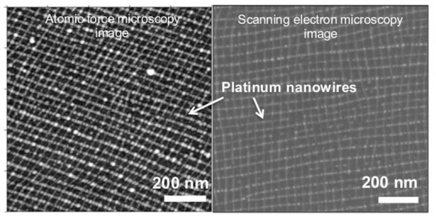
In FY16 we (1) successfully shear-aligned two layers of a block copolymer to produce a greater than 1-cm2 mesh of platinum nanometer-scale wires with approximately 10-nm diameters and 30-nm pitch by working with the commercially available block copolymer polystyrene and poly(2-vinylpyridine), where metal salts readily complex with the poly(2-vinylpyridine) phase (see figure); (2) determined that this nanowire mesh will be the basis of the negative-index metamaterial structure we aim to fabricate, which consists of alternating layers of metal and dielectric, but also has potential utility by itself as a conductive transparent electrode; (3) evaluated the optical and electrical properties of this nanowire mesh; and (4) built an apparatus to scale the shear alignment of block copolymers to the entire four wafers.


