Joshua D. Kuntz (15-ERD-043)
Abstract
Our project focused on the manipulation of the electromagnetic spectrum through the production of metamaterials. The goal was to interact with multiple wavelength bands of the electromagnetic spectrum concurrently to provide new materials for functional applications. The wavelengths varied from 250 to 400 nm (ultraviolet), 400 to 700 nm (visible), 700 to 20,000 nm (infrared), and 1 to 100 cm (microwave). The design of the structures with the ability to concurrently manipulate various wavelengths was inspired by structures found in nature, namely moth eyes. Moth eyes have hierarchical structures that minimize spectral reflections and maximize transmission, to provide optimal optical performance. The moth eye structure is made up of microscale topology (10–20 μm) with nanoscale topology (approximately 100 nm) on top. This biological structure exhibits excellent antireflection properties across the light spectrum. We designed and optimized a synthetic version of this structure in silicon and replicated the structure in flexible silicone. The hierarchical metamaterials consist of micrometer-scale pyramids 2–10 μm in size with nanoscale pyramids (10–100 nm) following the micrometer-scale surface. The performance of the hierarchical structure was excellent and closely matched modeling efforts. The hierarchical synthetic moth eye exhibited less than one percent reflection, both hemispherical and specular, from 250 to 2,500 nm. This performance extended to angles of incidence as high as 67 degrees. One of the important aspects of this work was the excellent agreement between the modeling of the performance of these structures and the measured values of reflectivity from the as-made surfaces. This enabled a set of design rules for tailoring of the properties of these optical structures.
Background and Research Objectives
Most optical components utilize antireflective coatings based on multilayered destructive interference to reduce surfaces’ reflectance. However, this principle of operation limits the efficacy of antireflective coatings to narrow wavelength ranges and angles of incidence. Thus, such antireflective coatings have only limited utility for many optical devices (such as solar cells and photodetectors) that require reduced reflectivity across broad wavelength regimes and angles of incidence. Furthermore, such antireflective coatings are most effective at reducing specular reflectance, but depending on the application, a reduction in the diffuse or hemispherical (sum of the diffuse and specular) reflectance may instead be desired. Because reflections occur whenever propagating light encounters a significant change in the index of refraction, an alternative antireflective approach is to create surfaces with a graded index of refraction. Such gradients can be simply created by texturing surfaces with structures so that the effective index of refraction varies from the tip to the base of the structure. High-aspect-ratio wires with nanometer- or micrometer-scale diameters are effective antireflective and light-trapping structures (Cai 2015; Fountaine 2016; Gervinskas 2013; Huang 2007; Srivastava 2010; Yalamanchili 2016). However, such high-aspect structures are also fragile and difficult to fabricate, which is problematic because the spectral response of such structures is highly sensitive to the exact tapering profile of nanowires (Diao 2016; Hua 2013; Huang 2013; Ji 2012; Jung 2010; Zhu 2009).
Alternatively, hierarchical metamaterial structures composed of two or more substructures that have different characteristic length scales and are stacked atop one another also effectively reduce reflectance. The design of the structures with the ability to concurrently manipulate various wavelengths was inspired by structures found in nature, namely moth eyes. Moth eyes have hierarchical structures that minimize spectral reflections and maximize transmission, to provide optimal optical performance. The moth eye structure is made of microscale topology (10–20 μm) with nanoscale topology (approximately 100 nm) on top. This biological structure exhibits excellent antireflection properties across the light spectrum. Because they do not require high aspect ratios to reduce reflectance, hierarchical structures can be simpler to produce. While the two different substructures introduce more design variables that can reduce optimization, they also provide enhanced tunability over the reflective properties of hierarchically structured surfaces.
Though a number of hierarchical antireflective structures have been demonstrated (Cho 2014; Choudhury 2013; Dudem 2016; Liu 201; Qi 2009; Tasmiat 2014), general guidelines for the design of hierarchical structures to attain desired antireflective properties are still lacking. We explored the parameter space of hierarchical structures to synthesize a set of guidelines relating how their structural parameters affect various aspects of their reflectivity, including the type of reflectivity (e.g., specular, diffuse, or hemispherical), its spectral response, and its angle dependency across the solar spectrum (250–2,500 nm). Because of the spectral regime we are targeting (i.e., ultraviolet, visible, and infrared light), our hierarchical structures are composed of substructures on the nanometer- and micrometer-length scales that we refer to as nanoarrays and microarrays, respectively. We determined that combining nanoarrays and microarrays, and tuning their dimensions and periodicity can affect the overall hierarchical structure's reflective response.
A significant portion of the work originally proposed for this project was dedicated to the production of hierarchical metamaterials directed to manipulation of the microwave portion of the electromagnetic (EM) spectrum. The work has been much slower to mature due to personnel availability and budget constraints.
Scientific Approach and Accomplishments
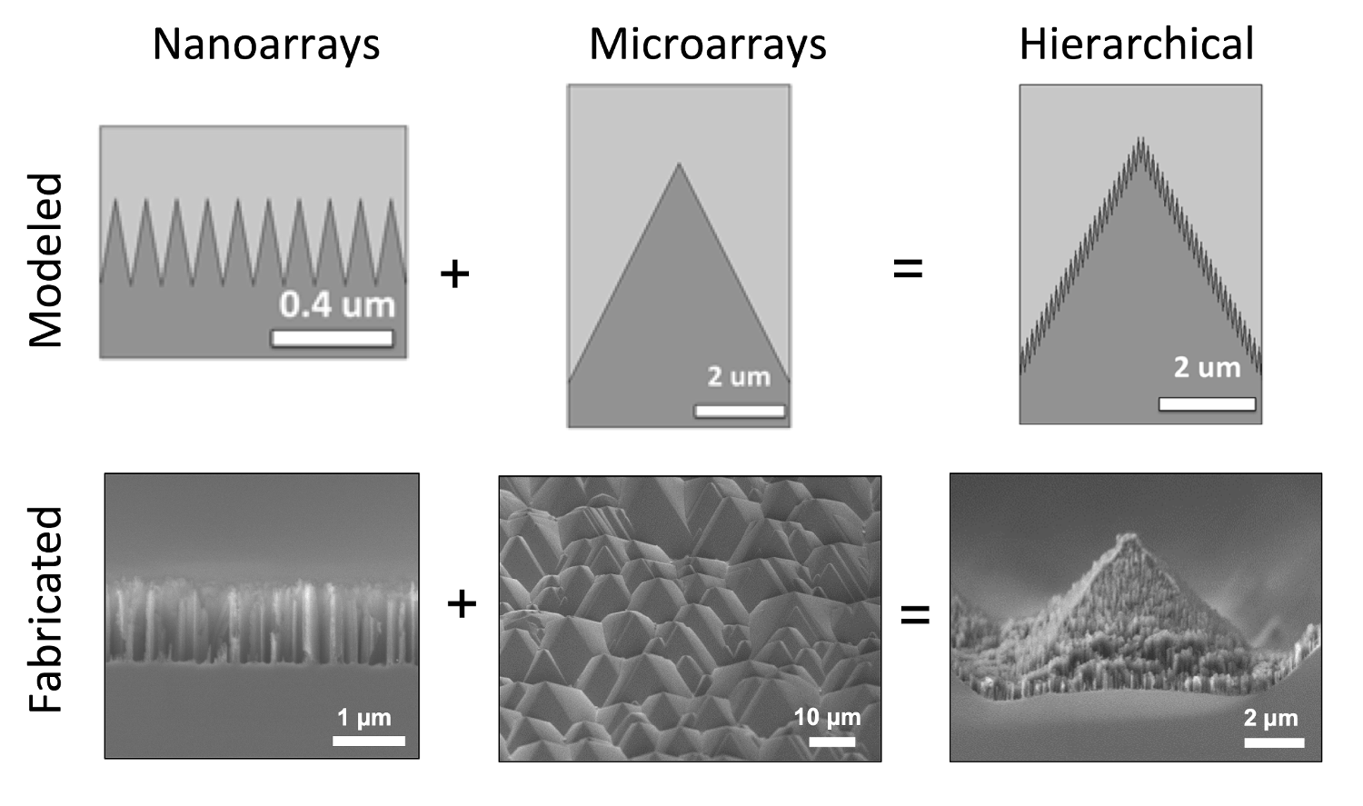
To understand the role of the micro- and nanometer-length-scale structures in reducing the reflectivity of hierarchical structures, we first studied the two length-scale structures individually. This was done by modeling the structures in COMSOL, a finite-element modeling software application with EM modules, and validating the model with experimental results by producing both microarrays and nanoarrays independently. In COMSOL, we modeled microarrays as triangles with a 5-µm base and height and modeled nanoarrays as yet smaller triangles that have a 100-nm base and 677-nm height. Experimentally, we fabricated nanoarrays of silicon nanowires by metal-assisted etching (MAE), and microarrays with crystallographically controlled potassium hydroxide (KOH) etching. Once validated, we continued the modeling and experimental work to produce the hierarchical metamaterial structures. Figure 1 shows how the nanoarrays and microarrays were combined to produce the hierarchical structures for the modeling and experimental work.
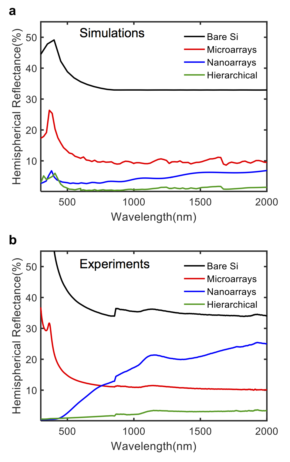
Our fabricated structures consisted of pyramids having comparable widths and heights of approximately 5.2 ± 3.3 µm and nanowires with heights of approximately 625 ± 122 nm and widths varying between approximately 50 and 200 nm. To produce microarrays consisting of pyramids, we subjected 100 silicon wafers to KOH-etching, a technique commonly used in the solar-cell industry to reduce silicon’s reflectance from approximately 34 percent to 10 percent (Dzhafarov 2013; Fan 2013; King 1991; Zubel 2000). To create the nanoarrays atop the silicon pyramids, silver nanoparticles were electrolessly deposited atop the silicon pyramids. The substrates were then subjected to 2 minutes of metal-assisted etching (MAE), during which silicon was etched preferentially where the metal was located, producing nanowires atop the silicon pyramids (Huang 2011). Figure 2 shows the calculated and measured hemispherical (i.e., total) reflectance of a bare silicon surface (black trace) and of the three structures of interest: microarrays (red trace), nanoarrays (blue trace), and hierarchical arrays (green trace).
To obtain a better understanding of the effects of the scale of the nanoarrays and the hierarchical structures we fabricated various thicknesses of each for comparison. This was done by controlling the etch time for the MAE procedure.
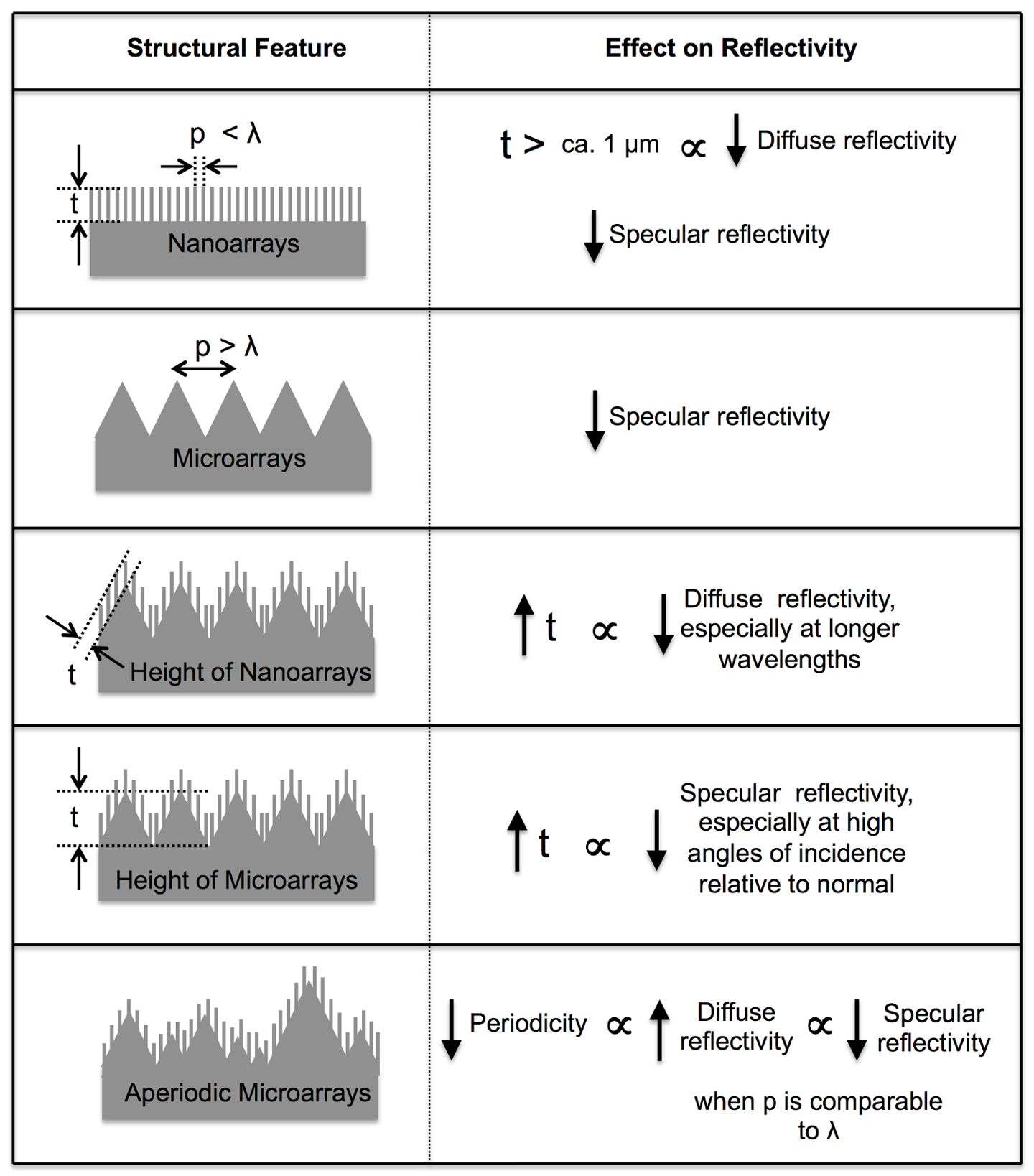
What was learned from the simulation and experimental results can be summarized graphically. Figure 3 depicts the effects of nanoarrays, microarrays, and hierarchical structures as a function of feature height and periodicity. Results from this led the team to explore two alternate routes to produce antireflective surfaces, block copolymer templates for controlling MAE and carbon nanotube (CNT) forest growth, both on aperiodic microarrays.
The hierarchical structures produced by block copolymer template MAE showed a modest improvement over the aperiodic hierarchical metamaterial structures. This improvement was best seen by lower hemispherical reflection values at shorter nanoarray heights. The CNT forest grown atop the aperiodic microarrays performed significantly better in all circumstances, particularly in lower specular reflections at high angles of incidence.
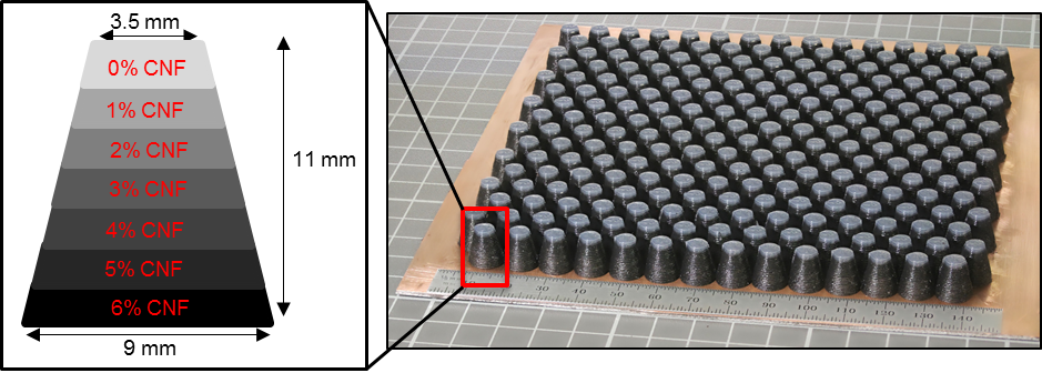
Microwave-wavelength metamaterials were also designed, modeled, and produced. These structures proved to be more complicated to fabricate and measure performance, so results are more sparse. Radio-frequency-shielding, carbon-based silicone formulations were developed and a direct-ink writing system was used to create flexible tunable structures. Simulations guided materials selection and the geometry/dimensions of structures. Direct ink writing is a three-dimensional (3D-) printing technique that extrudes material along a prescribed tool path. The ink is carefully formulated to enable the layer-by-layer building of a 3D structure. This technique is used to create novel geometries with tailored compositions. One of the microwave metamaterial designs can be seen in Figure 4, where both geometry and composition are concurrently changing.
Impact on Mission
Our project aligns well with the Laboratory's core competency in advanced materials and manufacturing. Broadband metamaterials have applications in a range of DOE's and Lawrence Livermore National Laboratory's mission areas, such as the use of sensors and lasers for applications in national and energy security. This project leverages the investments made toward additive manufacturing while creating new materials with optimized physical properties, other than mechanical.
Conclusion
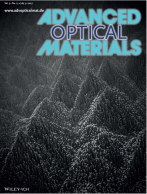
The performance of the hierarchical structure was excellent and closely matched modeling efforts. The hierarchical synthetic moth eye exhibited less than one percent reflection, both hemispherical and specular, from 250 to 2,500 nm. Remarkably, this performance extended to angles of incidence as high as 67 degrees. This work was published in Advanced Optical Materials and (Figure 5, Diaz Leon 2017).
Figure 5. Inside front cover from Advanced Optical Materials, showing a rendering of the project’s hierarchical synthetic moth eye structure (Diaz Leon 2017).
One of the most important results of this work was the excellent agreement between the modeling of the performance of these structures and the measured values of reflectivity from the as-made surfaces. This enabled a set of design rules for the tailoring of the properties of these optical structures.
References
Cai, J. and L. Qi. 2015. "Recent Advances in Antireflective Surfaces Based on Nanostructure Arrays. "Materials Horizons 2(1):37–53. doi: 10.1039/C4MH00140K.
Cho, S. J., et al. 2014. "Three-Dimensionally Designed Anti-Reflective Silicon Surfaces for Perfect Absorption of Light." Chemical Communications 50(99):15710–15713.
Choudhury, B. D., et al. 2013. "Silicon Micro-Structure and ZnO Nanowire Hierarchical Assortments for Light Management." Optical Materials Express 3(8):1039–1048. doi: 10.1364/OME.3.001039.
Diao, Z., et al. 2016. "Nanostructured Stealth Surfaces for Visible and Near-Infrared Light." Nano Letters 16(10): 6610–6616. doi: 10.1021/acs.nanolett.6b03308.
Diaz Leon, J.J., et al. 2017. "Design Rules for Tailoring Antireflection Properties of Hierarchical Optical Structures." Advanced Optical Materials 5(13):1700080. doi: 10.1002/adom.201700080.
Dudem, B., et al. 2016. "A Multifunctional Hierarchical Nano/Micro-Structured Silicon Surface with Omnidirectional Antireflection and Superhydrophilicity Via an Anodic Aluminum Oxide Etch Mask." RSC Advances 6(5):3764–3773. doi: 10.1039/C5RA22535C.
Dzhafarov, T., 2013. "Silicon Solar Cells with Nanoporous Silicon Layer," in Solar Cells - Research and Application Perspectives, ed. Arturo Morales-Acevedo (London: Intech, 2013). doi: 10.5772/3418.
Fan, Y., et al. 2013. "Differences in Etching Characteristics of TMAH and KOH on Preparing Inverted Pyramids for Silicon Solar Cells." Applied Surface Science 264:761–766. doi: 10.1016/j.apsusc.2012.10.117.
Fountaine, K. T., et al. 2016. "Near-Unity Unselective Absorption in Sparse InP Nanowire Arrays." ACS Photonics 3(10): 1826–1832. doi: 10.1021/acsphotonics.6b00341.
Gervinskas, G., et al. 2013. "Surface-Enhanced Raman Scattering Sensing on Black Silicon." Annalen der Physik 525(12): 907–914. doi: 10.1002/andp.201300035.
Hua, B., et al. 2013. "Rational Geometrical Design of Multi-Diameter Nanopillars for Efficient Light Harvesting." Nano Energy 2(5): 951–957. doi: 10.1016/j.nanoen.2013.03.016.
Huang, Y. F., et al. 2007. "Improved Broadband and Quasi-Omnidirectional Anti-Reflection Properties with Biomimetic Silicon Nanostructures." Nature Nanotechnology 2(12): 770–774. doi: 10.1038/nnano.2007.389.
Huang, Z., et al. 2011. "Metal-Assisted Chemical Etching of Silicon: A Review.". doi: 10.1002/adma.201001784.
Huang, Y. F. and S. Chattopadhyay. 2013. "Nanostructure Surface Design for Broadband and Angle-Independent Antireflection." Journal of Nanophotonics 7(1):073594–073594. doi: 10.1117/1.JNP.7.073594.
Ji, S., et al. 2012. "Improved Antireflection Properties of Moth Eye Mimicking Nanopillars on Transparent Glass: Flat Antireflection and Color Tuning." Nanoscale 4(15):4603–4610. doi: 10.1039/c2nr30787a.
Jung, J. Y., et al. 2010. "A Strong Antireflective Solar Cell Prepared by Tapering Silicon Nanowires." Optics Express 18 Supplement 3(19): A286–A292. doi: 10.1364/OE.18.00A286.
King, D. L.; Buck, M. E. 1991. In Experimental optimization of an anisotropic etching process for random texturization of silicon solar cells, 22nd IEEE Photovoltaic Specialists Conference, Las Vegas, NV, Oct. 7–10, 1991. p. 303.
Liu, Y., et al. 2014. "Hierarchical Robust Textured Structures for Large Scale Self-Cleaning Black Silicon Solar Cells." Nano Energy 3:127–133. doi: 10.1016/j.nanoen.2013.11.002.
Qi, D., et al. 2009. "Simple Approach to Wafer-Scale Self-Cleaning Antireflective Silicon Surfaces." Langmuir 25 (14): 7769–7772. doi: 10.1021/la9013009.
Srivastava, S. K., et al. 2019. "Excellent Antireflection Properties of Vertical Silicon Nanowire Arrays." Solar Energy Materials and Solar Cells 94(9):1506–1511. doi: 10.1016/j.solmat.2010.02.033.
Tasmiat, R., et al. 2014. "High Density Micro-Pyramids with Silicon Nanowire Array for Photovoltaic Applications." Nanotechnology 25(48):485202. doi: 10.1088/0957-4484/25/48/485202.
Yalamanchili, S., et al. 2016. "Enhanced Absorption and <1% Spectrum-and-Angle-Averaged Reflection in Tapered Microwire Arrays." ACS Photonics 3(10):1854–1861. doi: 10.1021/acsphotonics.6b00370.
Zhu, J., et al. 2009. "Optical Absorption Enhancement in Amorphous Silicon Nanowire and Nanocone Arrays." Nano Letters 9(1): 279–282. doi: 10.1021/nl802886y.
Zubel, I. 2000. "Silicon Anisotropic Etching in Alkaline Solutions III: On the Possibility of Spatial Structures Forming in the Course of Si(100) Anisotropic Etching in KOH and KOH+IPA Solutions." Sensors and Actuators A: Physical 84(1–2): 116–125. doi: 10.1016/S0924-4247(99)00347-7.
Publications and Presentations
Hiszpanski, A. M., et al. 2017. “Broadband and Omnidirectional Anti-Reflectivity of Hierarchically Structured Silicon.” MRS Spring Meeting, Phoenix, AZ, April 17–21, 2017. LLNL-PRES-729273.
Diaz Leon, J. J., et al. 2017. “Design Rules for Tailoring Antireflection Properties of Hierarchical Optical Structures.” Advanced Optical Materials 5(13):1700080. doi: 10.1002/adom.201700080. LLNL-JRNL-713005.


