Rebecca Nikolic (13-ERD-004)
Abstract
Our objective with this project was to develop an electrical power-generation device for space-based applications that combined fissile material with a three-dimensional semiconductor. This high-risk, potentially high-pay-off project used a three-dimensional design to utilize a large semiconductor volume, dramatically increasing the output power. Our design resulted in many milliwatts of output power rather than the microwatts achieved from two-dimensional surface-generation approaches using low-activity beta-generating radioisotopes. We focused on development of a three-dimensional platform for a radioisotope battery and the investigation of icosahedral boron phosphide as a radiation-hard semiconductor. We carried out a fundamental material science investigation on icosahedral boron phosphide and made progress on the epitaxially grown thin films using a gas composition of hydrogen, phosphine, and diborane. The optimized configuration determined during the course of this project for best crystal growth is on silicon carbide wafers with atomic steps toward the (1-100) plane. Based on these developments, the next steps for research are to fabricate a proof-of-principle battery using icosahedral boron phosphide and measure its output power.
Background and Research Objectives
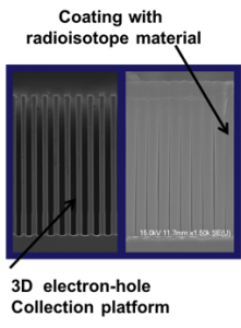
Spacecraft require an energy source that operates reliably and predictably for extended periods in harsh environments. For many years, the solution has been radioisotope power systems. Our objective with this project is to develop an electrical power-generation device for space-based applications that combines fissile material with a three-dimensional semiconductor to enable the use of a large volume of the semiconductor for power generation for dramatically increased power density, instead of limiting it to the surface, which provides only microwatt output power. We used innovative methods for dramatically increasing the power generation over current nuclear batteries by using a three-dimensional semiconductor structure coated with a high-activity alpha-producing radioisotope material, shown conceptually in Figure 1. Alpha radiation causes electron–hole pair generation inside the semiconductor, and produces more electron–hole pairs than beta radiation in any given semiconductor. The movement of these charges over time results in electronic current, and when connected to a load resistor, creates a power source.
In this project, we (1) achieved proof-of-principle current generation using a planar semiconductor structures coated with uranium oxide; (2) prepared three-dimensional semiconductor structures for template growth of icosahedral boron phosphide, conducted crystal growth of these films on various substrates, and investigated the effects of crystal orientation; (3) developed metal contacts for diode formation; and (4) worked towards developing a portfolio of intellectual property by submitting a patent application.1 Taken together, the progress we achieved in developing the three-dimensional radioisotope battery structure and the progress in growing icosahedral boron phosphide has provided the foundational work for device-level progress in this area.
Scientific Approach and Accomplishments
We developed a baseline radioisotope battery platform using planar silicon-carbide semiconductor diode material with a uranium oxide radioisotope top coating and characterized the output power and degradation mechanisms.2 Silicon carbide was chosen because of its high radiation hardness—the energy required to displace an atom from its lattice site is 21.8 eV, which is higher than most semiconductors. Apart from that, a low leakage current is available with its wide band-gap, which benefits the open circuit voltage of the radioisotope battery. The penetration depth of a 5-MeV alpha particle in silicon carbide is 16 µm (into bare silicon carbide). A thick intrinsic thickness of 100 µm of a commercial silicon carbide PIN diode allows all of the alpha energy to deposit in the active region. (A PIN diode has a wide, undoped intrinsic semiconductor region between a p-type semiconductor and an n-type semiconductor region—in other words, the intrinsic "i" region is flooded with charge carriers from the "p" and "n" regions.) Uranium oxide 232U3O8 was chosen because of its high energy-decay properties and half-life of 70 years. The half-life of 232U3O8 is suitably long enough for battery use, yet is short enough to obtain the high specific activity required for current generation. In addition, decay daughters also emit alpha particles that will generate more electron–hole pairs than by uranium decay alone.
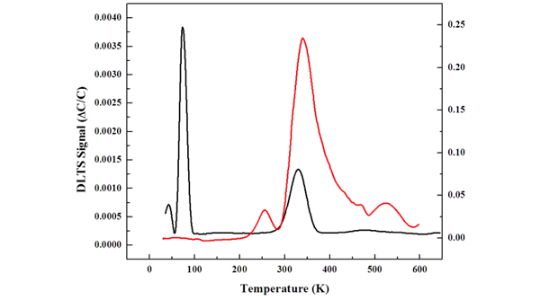
Because of the availability of uranium-233, we used this isotope for early experimentation. Specifically, we successfully developed a process for 233U3O8 deposition, which used electrochemical deposition from an isopropanol solution and produced very uniform thin films. Using the silicon carbide PIN diode with a uranium oxide coating, we measured the current generation over time and found that the output current dropped during irradiation. The high-energy alpha particles create point defects (an interstitial atom or vacancy) in the silicon carbide. These point defects combine with intrinsic defects, impurities, or dopants in the silicon carbide material to form stable deep-level complexes. The deep-level traps serve as recombination centers where generated electron–hole pairs recombined to reduce the short circuit current. The radiation-induced defects can also capture the majority carriers to make the semiconductor more resistive. The activation energy, cross section, and defect density can be resolved by deep-level transient spectroscopy, an experimental tool for studying electrically active defects in semiconductors. The spectra of a silicon carbide diode obtained by deep-level transient spectroscopy before and after a 5-MeV alpha irradiation are shown in Figure 3. In this instance, the alpha source used was 1-mCi polonium-210 and the irradiation time was 4.5 hours.
After irradiation, the signals of shallow-level defects that peaked at 40 and 70 K were annihilated. This could be attributed to the removal of donor-type impurities that combine with point defects to form deep-level complexes. A new defect-level of 0.5 eV was found at 250 K. The initial deep-defect level of 0.62 eV that peaked at 330 K was increased by 2.5x and broadened after irradiation. Because of the semiconductor output power degradation, an added research approach of investigating icosahedral boron phosphide, which is purported to be radiation hard, was pursued.3,4
Because bulk substrates of icosahedral boron phosphide are unavailable, the material must be grown on non-native crystalline substrates. Several approaches to icosahedral boron phosphide epitaxial growth were employed to modulate and improve the film quality on conventional planar substrates, substrates with engineered surface steps, and novel three-dimensional structures. Growth of icosahedral boron phosphide was performed using a cold-walled chemical vapor deposition chamber using diborane and phosphine in ambient hydrogen on planar silicon carbide, planar aluminum nitride on sapphire, and three-dimensional silicon carbide pillars.
We selected planar silicon carbide as a potential substrate because of the low lattice mismatch to icosahedral boron phosphide (2.5%), its commercial availability, its chemical stability under icosahedral boron phosphide growth conditions, and the potential to make a hetero-structure diode. By taking x-ray rocking curves to measure the crystal quality, we determined that the optimal growth temperature of icosahedral boron phosphide over the temperature range of 1,250 to 1,450°C was 1,300°C, with a rocking curve full-width-at-half-maximum value of 1,080 arcsec.5,6 Industry-standard silicon carbide substrates have atomic steps towards the [11-20] crystal direction. Because these steps strongly influence the nucleation of the icosahedral boron phosphide film, modifying the surface steps can modulate the growth of the film. When changing the crystallographic directions of the steps from the standard [11-20] direction to a custom [1-100] direction at the optimal growth temperature, rotational twin domains in molecular hydrogen (a type of crystallographic defect) were reduced from a density of 30% on a standard silicon carbide substrate to less than 1% on the custom substrate.5,7 This reduction in crystal defects will improve the electronic transport of charge carriers through the material, a necessity for reliable diode fabrication and performance.
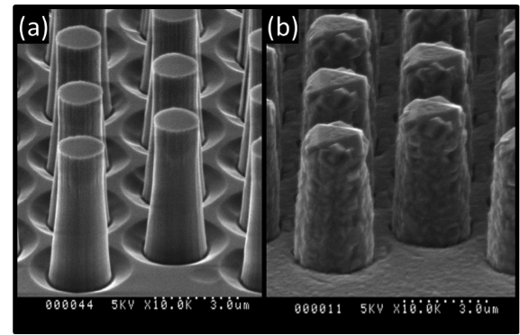
Aluminum nitride on sapphire templates was also selected as a planar substrate. Similar to silicon carbide, the lattice mismatch is low (3.7%) and has good chemical stability above 1,200°C in molecular hydrogen. Icosahedral boron phosphide films grown at 1,250°C have a lower silicon impurity background than comparable films grown on silicon carbide. Thus, aluminum nitride substrates may be more suitable than silicon carbide for growing higher-purity icosahedral boron phosphide films. To further the goal of creating three-dimensional devices, we explored nonplanar substrates. Advanced epitaxy on three-dimensional structures and templates has the potential to create three-dimensional heterostructure diodes, and may also be used to control and terminate certain types of crystal defects and effects from stress that arise from growing one material on top of another.8 We developed a process for producing large arrays of silicon carbide microscopic pillars for creating template substrates. The pillars were fabricated by patterning a silicon carbide wafer using photolithography and then plasma etching using an electron cyclotron resonance, high-intensity plasma etcher with sulfur hexafluoride gas. Bare 2-μm-diameter and 5-μm-tall silicon carbide pillars are depicted in Figure 4(a). Figure 4(b) shows a icosahedral boron phosphide film grown conformably around the pillars. The pillars tops are capped with a large singular triangular crystal, while the sidewalls are polycrystalline. By growing discrete crystals on each pillar, lateral stresses can be relaxed because the strain is confined to the pillar tops instead of over large planar areas. Thus far, the thickness of planar icosahedral boron phosphide films has been limited by stress-induced cracking. Results show that we have achieved discrete crystal growth, which we expect to enable thicker film growth.
Although forming low-resistance ohmic contacts is challenging for many wide band-gap materials, such as icosahedral boron phosphide, these types of metal contacts are an essential element of a diode. So, as a requisite step prior to fabricating and characterizing icosahedral boron phosphide diodes, we developed ohmic metal contacts to icosahedral boron phosphide using chromium–platinum and nickel–gold metal layers.9,10
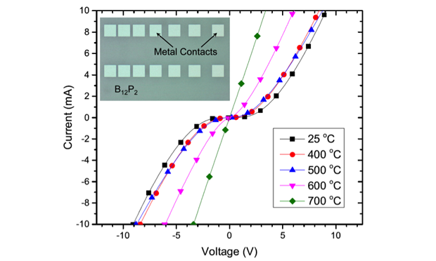
Icosahedral boron phosphide was first grown epitaxially on a semi-insulating silicon carbide substrate by chemical vapor deposition. We then used photolithography and electron-beam evaporation to pattern metal contacts in a transfer-length model arrangement. Figure 5 (inset) shows a typical pattern. The patterned contacts were annealed at increasingly higher temperatures, while current and voltage measurements were taken at room temperature between each anneal.
Contacts of chromium–platinum (of layers 50- and 100-nm thick, respectively) became ohmic after annealing at 700°C for 30 seconds, evidenced by the transition from a nonlinear to linear current–voltage relationship (see Figure 5). The specific contact resistance was 2 x 10⁻⁴ Ωcm2. Contacts of nickel–gold (layered 100-nm thick) were ohmic prior to any annealing and reached a minimum specific contact resistance of 1 to 4 x 10⁻⁴ Ωcm2 after annealing over the temperature range of 500 to 800°C. Rutherford backscattering spectrometry revealed a strong reaction and intermixing between chromium–platinum and icosahedral boron phosphide at 700°C, and a reaction layer between nickel and icosahedral boron phosphide thinner than about 25 nm at 500°C. Nickel–gold contacts displayed superior properties compared to chromium–platinum contacts, including ohmic conduction prior to annealing, better thermal stability, and a similar contact resistance at lower anneal temperatures.
Impact on Mission
This technology enables development of long-term emplaced sensors in a wide variety of missions of interest to NNSA and other federal agencies. Our research was also closely aligned with Laboratory missions in advanced materials and manufacturing and actinide sciences, as well as enabling new energy sources for military applications.
Conclusion
Small nuclear batteries, depending on the application and power, could become an off-the-shelf power-supply item, enabling long-term use of micro-powered devices and sensors capable of uninterrupted operation for decades. In addition, higher-power batteries will enable deep-space probes to operate with a smaller size and weight budget than conventional nuclear power supplies. Toward that end, we carried out fundamental material science work on icosahedral boron phosphide as a building block for a three-dimensional radioisotope battery. We made progress on the epitaxially grown thin films using a gas composition of hydrogen, phosphine, and diborane, and conducted epitaxial growth on silicon carbide, aluminum nitride, and template pillars of silicon carbide wafers. We determined that the optimized configuration for best crystal growth is on silicon wafers with atomic steps moving toward the [1-100] plane, which resulted in an x-ray rocking curve full-width-at-half-maximum value of 1,080 arcsec. Metal contacts were also developed and had a low specific contact resistance of 1 to 4 x 10⁻⁴ Ωcm2 using nickel–gold (100 nm/100 nm) and chromium–platinum (50 nm/100 nm) metal stacks. Using these developments, the next step for this research is to fabricate a proof-of-principle battery using icosahedral boron phosphide and measure its output power. Finally, by coating three-dimensional semiconductor structures, such as icosahedral boron phosphide or commercially available silicon carbide, with a properly selected radioisotope, high output power is possible. To further develop this area, our follow-on work will pursue the creation of wide band-gap semiconductors coated with select radioisotopes and arranged in a three-dimensional platform.
References
- Nikolic, J., et al., Three dimensional radioisotope battery and methods of making the same. U.S. Appl. 14/214,244 (Mar. 14, 2014).
- Stoyer, M. A., et al., Simulations of novel nuclear battery concepts. 247th ACS National Mtg. and Exposition, Dallas, TX, Mar. 16–20, 2014. LLNL-PRES-651894.
- Carrard, M., D. Emin, and L. Zuppiroli, “Defect clustering and self-healing of electron-irradiated boron-rich solids." Phys. Rev. B 51(17), 11270 (1995).
- Emin, D., "Unusual properties of icosahedral boron-rich solids." J. Solid State Chem. 179(9), 2791 (2006).
- Frye, D., et al., Epitaxial icosahedral boron phosphide grown on vicinal (0001) 4H-SiC substrates. 20th American Conf. Crystal Growth and Epitaxy, Big Sky, MT, Aug. 2–7, 2015. LLNL-ABS-668428.
- Frye, D., et al., Growth of B12P2 on 4H-SiC. (In preparation).
- Frye, D., et al., Suppression of rotational twinning in epitaxial B12P2 grown on 4H-SiC substrates tilted to the (1-100). (In preparation).
- Falub, V., et al., “Scaling hetero-epitaxy from layers to three-dimensional crystals.” Science 335(6074), 1330 (2012).
- Frye, C. D., et al., Cr/Pt and Ni/Au ohmic contacts to B12P2. Electronic Materials Conf., Santa Barbara, CA, June 25–27, 2014. LLNL-PRES-656119.
- Frye, C. D., et al., "Sintered Cr/Pt and Ni/Au ohmic contacts to B12P2." J. Vac. Sci. Tech. 33, 031101 (2015). LLNL-JRNL-666166.
Publications and Presentations
- Frye, C. D., et al., Cr/Pt and Ni/Au ohmic contacts to B12P2. Electronic Materials Conf., Santa Barbara, CA, June 25–27, 2014. LLNL-PRES-656119.
- Frye, C. D., et al., Epitaxial icosahedral boron phosphide grown on vicinal (0001) 4H-SiC substrates. 20th American Conf. Crystal Growth and Epitaxy, Big Sky, MT, Aug. 2–7, 2015. LLNL-ABS-668428.
- Frye, C. D., et al., "Sintered Cr/Pt and Ni/Au ohmic contacts to B12P2." J. Vac. Sci. Tech. 33, 031101 (2015). LLNL-JRNL-666166.
- Stoyer, M. A., et al., Simulations of novel nuclear battery concepts. 247th ACS National Mtg. and Exposition, Dallas, TX, Mar. 16–20, 2014. LLNL-PRES-651894.


