Aiden Martin (16-FS-037)
Abstract
Boron-containing materials are increasingly drawing interest for use in laser targets, quantum photonics, electronics, optics, and high-temperature and reactive chemical environments. These important applications are, however, overshadowed by fabrication challenges arising from instabilities produced during the thermally induced fabrication process. Other critical hurdles in fabrication of thick, continuous boron and boron-carbide films include typically slow growth rates and the difficulty of controlling film stoichiometry and surface roughness.
Electron-beam-induced deposition (EBID) is a rapidly developing technique that has been demonstrated for a wide range of materials (Utke et al. 2012). EBID avoids thermal- and mass-transport-related instabilities by overcoming the activation barrier for material deposition by electron-induced dissociation of adsorbed precursor molecules. This feasibility study designed and implemented a large-area EBID platform for the study of boron-film deposition. The system enabled deposition of boron-containing material with a minimum depositional cross-section of approximately 500 µm in diameter. We used trimethyl borate (TMB) as the EBID precursor because its chemical structure and handling requirements are similar to those of conventional EBID precursors, making it ideal for verification of the EBID platform. Deposition using TMB as the precursor was investigated as a function of substrate temperature, which showed temperature-dependent deposition rates and stoichiometry changes in the deposited material. Phenylboron dichloride (PBDC) was studied as the EBID precursor because it is oxygen-less and analogous to the conventional chemical-vapor deposition (CVD) precursor BCl3. By utilizing PBDC as the precursor, BC3 material was realized via EBID. Future endeavors to realize stoichiometric B4C and pure boron films by EBID will require implementation of improved vacuum technology and gas-handling systems. The identification of PBDC as a boron-carbon source could prove critical in future CVD studies by providing a pathway for B4C deposition via a relatively benign precursor. Our research has introduced a new material-fabrication method to Lawrence Livermore National Laboratory and developed novel processes for deposition of boron-containing films.
Background and Research Objectives
Electron-beam-induced deposition (EBID) is a rapidly developing technique that has been demonstrated for a wide range of materials (Utke et al. 2012). It entails electron dissociation of precursor surface adsorbates into fragments that react with a solid surface. Deposition occurs when the reaction products are non-volatile, resulting in the addition of surface material comprised of precursor-molecule constituents. The process has major advantages over thermal chemical vapor deposition (CVD) processes. For example, EBID is performed at or close to room temperature by injecting a precursor gas into a high-vacuum or ultra-high-vacuum chamber, while a substrate is irradiated by an energetic (1–300 keV) electron beam. In this way, the substrate is not exposed to the elevated temperatures required for the thermal decomposition of precursor molecules. Exposure to elevated temperatures is incompatible with commonly used mandrels for the deposition of Inertial Confinement Fusion (ICF) capsules and leads to the development of undesirable stresses that can cause film cracking and delamination.
Currently, no boron-containing material has been deposited using the EBID process. Other research groups exploring the use of EBID are primarily focused on depositing material for applications in the semiconductor industry, including lithography mask repair and nanoscale fabrication. Materials generally studied include carbon nanowires, silica-based insulating layers, and a wide range of metals. Previous research has demonstrated efficient deposition of continuous films on the nano to micro scales.
The goal of our study was to provide the first demonstration of a macroscopically large area boron-based EBID process that is scalable to high-energy-density (HED) and ICF target-fabrication requirements. A significant scientific offshoot of this research is an expansion of the possible boron precursors that can be directly applied to thermal CVD. Wider acceptance of CVD to deposit boron structures such as nanotubes is hampered by boron's toxicity and reactivity concerns. For boron materials to achieve the same scientific and technological impact as materials such as graphene and carbon nanotubes (which can be made from simple alcohols), boron-based fabrication methods must be safe, widely accessible, and scalable to mass production.
Scientific Approach and Accomplishments
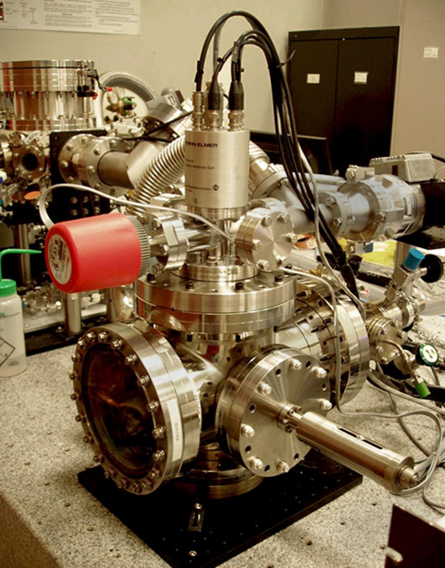
Currently, there are no EBID instruments available that enable boron deposition at adequate rates with beam sizes greater than 10 µm. As part of this project, we designed and constructed a large-area EBID platform (Figure 1) with the following specifications and capabilities: (1) provide an electron-beam diameter of greater than 500 µm, (2) enable in situ heating of the substrate, (3) incorporate a high-purity gas-injection system for precursor delivery, and (4) simultaneously maintain a gaseous environment in the substrate region and high vacuum pressure in the electron-source region.
Figure 2a is a schematic diagram of the final configuration of the EBID platform constructed at the Laboratory; its implementation is shown in Figure 2b. The electron optics (a 5-keV electron flood gun) are separated from the substrate chamber by differential pumping; electrons are steered through a set of 1.5-mm apertures into the chamber. Using this configuration, the pressure in the electron source is maintained at 10-5 Torr while the chamber pressure is maintained at approximately 5x10⁻² Torr. The optimum electron-beam settings were determined by measuring the electron-beam current as a function of electron energy. The optimal conditions used during our experiments were an operating electron energy of 2 keV and a focused Gaussian profile that provided maximum electron flux.
Trimethyl borate (TMB) was identified as the ideal EBID precursor for this research because it has similar structural properties to those of tetraethyl orthosilicate (TEOS) precursor, which has been thoroughly studied for use in the EBID process to deposit silica films. Experiments with TMB (B(OCH3)3) were performed as a function of substrate temperature to determine the deposition rate, crystallinity, and stoichiometry of the films deposited by EBID.
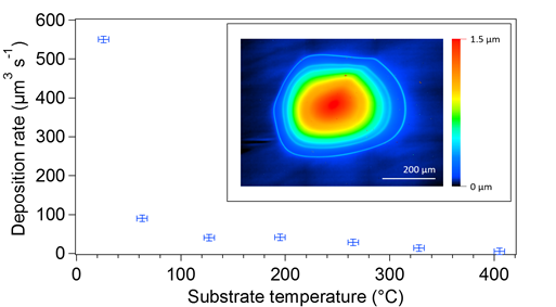
The graph in Figure 3 shows the deposition rate on silicon as a function of substrate temperature using a 2 keV, approximately 18 µA, 140 µm Gaussian beam radius electron beam. Height profiles (Figure 3 inset) were collected using a Keyence VK-X100 laser-scanning confocal microscope. Material was efficiently deposited at room temperature and the rate sharply decreased (Figure 3, blue error bars) with increasing substrate temperature due to a decrease in precursor surface-coverage on the substrate. Energy-dispersive x-ray spectroscopy (EDS) was performed using a Phenom ProX scanning electron microscope at 5 keV electron energy to determine the composition of the deposited material. At room temperature, the atomic composition of the material is 20 percent boron, 25 percent carbon, and 55 percent oxygen. The concentration of boron and oxygen decreases with increasing substrate temperature, while the carbon concentration increases. Carbon deposited at higher temperatures was caused by electron-induced dissociation of residual hydrocarbons in the substrate chamber.
The results obtained using the TMB precursor validated the performance of the Laboratory’s EBID deposition platform; however, pure boron or boron-carbide material was not realized. During this project, the novel precursor phenylboron dichloride (PBDC, C6H5BCl2) was identified. Use of this precursor removed the problem of incorporation of oxygen into the final material from the precursor. Previous electron-dissociation studies obtained favorable reaction cross-sections. Experiments using the PBDC precursor were performed as a function of substrate temperature to determine the deposition rate, crystallinity, and stoichiometry of the films deposited during the EBID process.
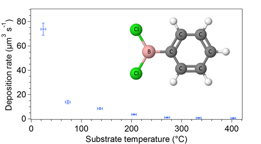
The graph in Figure 4 shows the deposition rate as a function of substrate temperature using a 2 keV, approximately 11.7 µA, 140 µm Gaussian radius electron beam. Material was clearly resolvable at room temperature, but the deposition rate was considerably reduced as substrate temperature increases. EDS analysis determined that the oxygen atomic concentration of the film was approximately 13 percent at room temperature, with boron, carbon, and chlorine concentrations of 23, 59, and 5 percent, respectively. The results are significant in that they show that PBDC is an efficient source of boron material; however, the ideal B4C system was not realized. Future work with other boron-precursor candidates will be required.
Impact on Mission
The design and construction of a new EBID instrument, and the development of a novel method for the study of boron-film deposition both support the Laboratory’s core competency in advanced materials and manufacturing to tackle the scientific and engineering challenges of accelerating the design, fundamental understanding, and deployment of new materials and manufacturing processes. Our research work also supports the Laboratory's mission focus area of stockpile stewardship science by providing new materials for high-energy-density research. The EBID method will be evaluated at the Laboratory for production of targets for future HED and ICF experiments that are beyond the capabilities of current techniques.
Conclusion
During this study we designed and constructed a large-area EBID platform for the study of boron-film deposition with the intention that it should also be used for future material-systems research at the Laboratory. Prior to this study, deposition of boron material using the EBID process was unexplored. Two novel precursor systems were investigated: trimethyl borate (TMB) and phenylboron dichloride (PBDC). The TMB precursor was found to incorporate significant amounts of oxygen into the final film, while the PBDC incorporated relatively minor concentrations of oxygen and chlorine while depositing boron and carbon at an atomic ratio of one to three. This feasibility study is the first step toward realizing pure boron and boron-carbide films using the EBID process; however, further work is required to decrease oxygen concentration in the films and improve stoichiometry toward B4C material.
The project has enabled collaborations with commercial (FEI Company) and academic (University of Technology, Sydney, Australia) institutions. The nanofabrication research capabilities of these institutions provide an ideal conduit for enabling other techniques for target fabrication. A patent (application submitted) describing the boron EBID methods will be leveraged for further research through industry collaboration. The identification of PBDC as a source of boron–carbon material could prove critical in future thermal-based CVD studies by providing a pathway for B4C deposition via relatively benign precursors. This work has introduced a new material-fabrication method to the Laboratory and developed novel processes for deposition of boron-containing films.
References
Utke, I., et al, eds. 2012. Nanofabrication Using Focused Ion and Electron Beams: Principles and Applications. New York: Oxford University Press.


