Adam Conway (16-FS-039)
Abstract
The main principle behind a photoconductive semiconductor switch (electrical conductivity that is affected by exposure to light) is internal conductance that is linearly proportional to the amount of absorbed light. In the “off” state, the device blocks electrical current and maintains charge voltage in the circuit because of its high resistance. In the “on” state (under optical excitation), the device conducts current and transfers charge voltage into the load. Current switch technology developed at Lawrence Livermore for use in megawatt-class radio-frequency power generation utilizes vanadium-doped silicon carbide, which enables exceptional standoff voltages, high currents, linear response, rapid on and off, and a wide range of frequencies in a chip that is 10 × 10 × 1 mm in size. With this technology, sub-bandgap light (532 nm) can uniformly illuminate the bulk of the switch, effectively turning on materials that are 1-mm thick or more. The tradeoff for uniform absorption, however, is a very low absorption coefficient, and thus most of the incident light is not converted to electrical current. In contrast, a total internal-reflection concept allows the light to bounce around inside the switch, effectively increasing the path length by greater than tenfold, thus allowing it to be absorbed more efficiently while maintaining a uniform profile. We have determined that our total internal-reflection concept is not only feasible, but increases the fraction of incident light absorbed from approximately 3% in the axial configuration to greater than 97% using total internal reflection. Additionally, the photo-to-electrical conversion in fabricated total internal-reflection switches was increased by fivefold. Furthermore, we demonstrated that we can image the absorption pattern within the switch using Fourier transform infrared spectroscopy, a technique that is used to obtain an infrared spectrum of absorption or emission of a solid, liquid, or gas. Finally, we demonstrated that diamond does show photoconductive response to 532-nm light in a proof-of-concept device.
Background and Research Objectives
One of the fundamental building blocks of power electronics is the semiconductor switch. Standard semiconductor power switches span a wide range of applications, power levels, and operating frequencies—the limits of which are primarily governed by intrinsic material properties such as speed of electron transport and breakdown electric-field strength. Traditionally, there has been a trade-off between speed (maximum operating frequency) and output power. Optically activated devices have the largest potential for high-power, high-frequency switching because they overcome the major problems of electrically triggered junction devices: jitter, slow opening and closing times, low repetition rates, and slow recovery times. Most types of optically activated devices, however, still rely on charge excitation in the depletion region of a semiconductor junction (~10 µm) and are thus limited in their blocking-voltage capabilities. This problem is solved in our device by using thick (1-mm) semi-insulating material that provides easy scalability for high-power systems. The principle behind the operation of such devices is that in the off state, the whole bulk of the device is used to block electric current and maintain charge voltage in the circuit. In the on state, the device conducts current under optical excitation and transfers charge voltage into the load. Devices based on this principle have been made using silicon and gallium arsenide, but were intrinsically limited by low critical fields and other intrinsic properties of these low-bandgap semiconductors. In the last decade, a renewed interest in photoconductive semiconductor switch was fueled by advancements in growth of high-quality wide-bandgap semiconductors. Our current technology, as well as developments of several external researchers, is focused on silicon carbide because of the superior set of properties (e.g., the critical field being second highest to diamond) and availability of semi-insulating wafers with low defect concentrations. Contrary to the external researchers, we have focused on sub-band excitation of vanadium deep levels in this material, allowing us to achieve uniform device illumination and very fast switching times. This choice in combination with other relevant technological developments produced record-breaking switches (standoff voltages of >30 kV and on currents of >1 kA per device). We are in a unique position to target radio-frequency power at gigahertz frequencies, approaching a power level at frequencies previously only attainable using vacuum tube technology. Nevertheless, one of the main drawbacks of our current approach is low (<1%) light utilization in the axial pump configuration. With this feasibility study, we investigated a conceptually new total internal-reflection design to potentially eliminate these problems.
Scientific Approach and Accomplishments
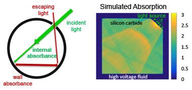
We addressed the issue of low light utilization to determine the feasibility of improving the size, weight, and power of an LLNL-demonstrated radio-frequency power-generator system using wide-bandgap silicon carbide photoconductive semiconductor switches. The current axially pumped switch design utilizes about 1% of the light because of the low absorption coefficient and short optical path length. This necessitates very high laser radiant energy, which degrades the metal contacts on the switch and can damage the fiber optics delivering light to the switch. We investigated the feasibility of a new design in which the light is introduced efficiently through a 45° notch to create total internal reflection that traps the light within the silicon carbide where it is absorbed (Figure 1). Our simulations show this new structure can potentially result in a greater than fifty-fold increase in light absorption over the axial design, while maintaining high voltage standoff with drastically improved reliability.
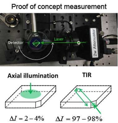
To investigate this experimentally, we used a continuous-wave 532-nm laser and a series of photodetectors to measure the amount of light absorbed in our device when illuminated in different ways (Figure 2). This resulted in an increase in absorption from about 3% in the axial configuration to over 97% in the total internal-reflection configuration. This equates to a 33-times increase. Switches with electrical contacts were also fabricated on silicon carbide substrates that enabled photo-induced electrical current to be measured in both the axial and total internal-reflection configuration using a 5-mW continuous-wave 532-nm laser. In the axial configuration, a photocurrent of 1.1 × 10⁻⁷ A at 100 V was measured, compared to the total internal-reflection configuration that had 5.5 × 10⁻⁷ A at 100 V. This is a five-times increase in photocurrent, which is a very encouraging preliminary result.
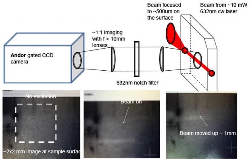
As described in the previous section, several of the main principles of the total internal-reflection concept were demonstrated by using the collimated laser light. Such illumination produces characteristic reflection patterns within a semiconductor die that are dependent on the beam input angle. Effective use of the total internal-reflection concept in photoconductive switching requires, however, a homogeneous carrier distribution. It is expected that most optimization towards the homogeneous excitation can be achieved by using specific notch designs and external beam shaping. Main design directions can be suggested by the ray-tracing modeling, but also require experimental feedback and verification. Current measurements lack necessary spacial resolution and sensitivity as an experimental verification. An alternative approach could be imaging of optical signals proportional to the generated carrier concentration. Photoluminescence from carrier recombination would be an obvious candidate, but silicon carbide as an indirect bandgap semiconductor produces negligible photoluminescence signals at room temperature. We demonstrated, nevertheless, that room-temperature Raman signals can be utilized for this purpose, as shown by images of the switch surface with and without an excitation beam propagating along the switch (Figure 3).
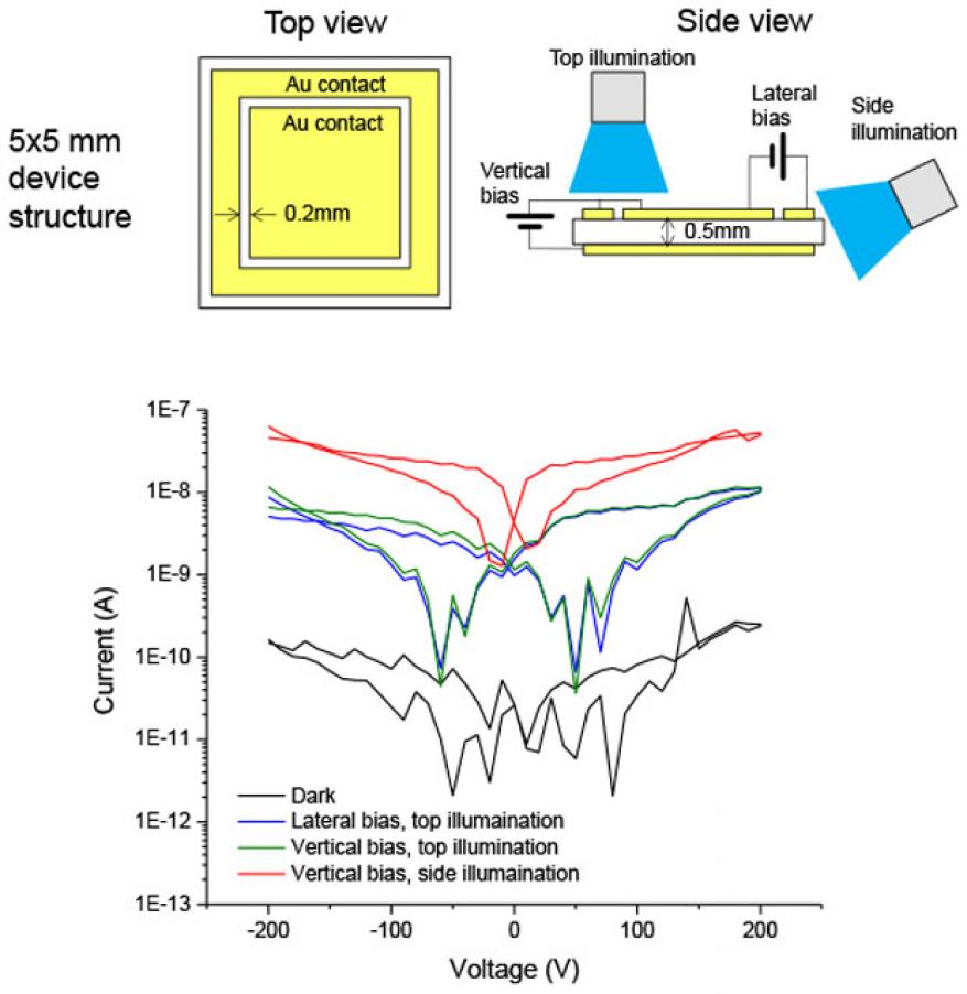
Finally, we determined that diamond is a superior material to silicon carbide because of the higher critical electric field, higher thermal conductivity, and higher carrier motilities. Use of diamond in a total internal-reflection concept requires, however, sub-bandgap excitation wavelengths. We demonstrated photocurrent generation using the polycrystalline diamond sample with nitrogen doping. The results, shown in Figure 4, show that currents 2 to 3 orders of magnitude larger than the dark current value are produced by the moderately powered 452-nm laser (2.7-eV wavelength at <<5.5 eV of diamond bandgap). Substantial increase of the photoconductive signal during the side illumination also suggests low absorption utilization and perfect fit for the total internal-reflection concept. Exact diamond grade and doping will have to be adjusted for generation of maximum powers.
Impact on Mission
Our photoconductive switch technology has the potential for use in high-radio-frequency power generation at significantly reduced system size and weight as well as increased power, which could enable new applications in support of cyber security, space, and intelligence for a compact communications microwave transmitter or high-power microwave-directed energy, as well as a novel compact laser design in support of the Laboratory's core competency in lasers and optical science and technology. Our study is most directly aligned with the advanced materials and manufacturing core competency—we are proposing a novel manufacturing design enabled by the Laboratory's micro-fabrication capability to create total internal-reflection semiconductor photoconductive switches using specially doped silicon carbide substrates.
Conclusion
During this LDRD feasibility study, we determined that our total internal-reflection concept is not only feasible, but increases the fraction of incident light absorbed from approximately 3% in the axial configuration to greater than 97% using total internal reflection. Additionally, the photo-to-electrical conversion in fabricated total internal-reflection switches was increased by fivefold. Furthermore, we demonstrated that we can image the absorption pattern within the switch using Fourier transform infrared spectroscopy. Finally, we used a proof-of-concept device to demonstrate that diamond does show photoconductive response to 532-nm light. This work has paved the way to future refinement of this total internal-reflection photoconductive switch using wide-bandgap semiconductors.


