Mark Converse (14-ERD-064)
Abstract
For many applications, it is desirable to create artificial materials with properties not found in nature (metamaterials) whose material performance is based on electromagnetic and mechanical microstructures. For electromagnetic materials, properties could include negative values of permittivity, permeability, or index of refraction. Mechanical properties of interest include low density, high stiffness, fracture strength versus stiffness, or even a specified stress-versus-strain curve. For this project, our purpose was to examine new paradigms where material performance is based on tightly coupled electromagnetic and mechanical microstructures, which could have wide-reaching effects on radar and communications system design, device miniaturization, and advanced sensor design. Specifically, we wanted to design and build electromagnetic metamaterials based on mechanical metamaterial substrates. This would both demonstrate the feasibility of coupling the functional performance of materials in the electromagnetic materials and mechanical regimes, and physically realizing electromagnetic metamaterials that have, to date, been mostly laboratory-based novelties. We began with one-dimensional anisotropic electromagnetic metamaterials, moved to three-dimensional isotropic electromagnetic metamaterials, and finally constructed materials designed for electromagnetic permittivity on mechanical metamaterial substrates. While not all the tasks were successful, we gained insights and increased capabilities for future work.
Background and Research Objectives
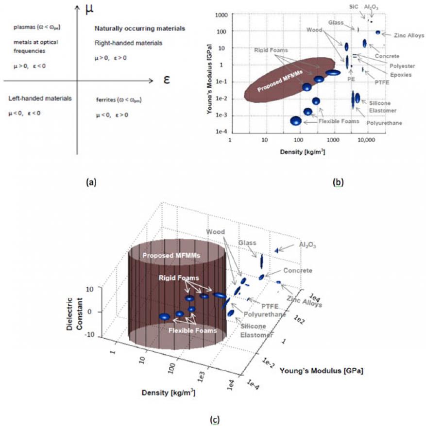
The goal of this project was to design and fabricate multifunctional metamaterials using the Lawrence Livermore's unique additive manufacturing capability. Our plan was to examine new paradigms where material performance is based on tightly coupled electromagnetic and mechanical microstructures. By designing and fabricating materials optimized for both microwave and mechanical properties, we explored the potential to create new materials spanning the large range shown in Figure 1(c). This would be done using simulation and numerical optimization to design novel metamaterials. We used materials fabricated using LLNL's unique additive manufacturing capability, and material samples were tested to verify the paradigm.
Metamaterials are artificial materials with properties not found in naturally occurring materials. For electromagnetic materials, this could be negative values of permittivity, permeability, or index of refraction, shown in Figure 1(a). Mechanical properties of interest include low density shown in Figure 1(b), high stiffness (Young’s modulus), fracture strength versus stiffness, or even a specified stress-versus-strain curve. Our goal was to vastly open the material space in the Ashby diagram shown in Figure 1(c), by combining electromagnetic and mechanical microstructures in novel ways.
For purposes of this study, we focused on multifunctional metamaterials that have interesting electromagnetic properties in the low gigahertz-frequency spectrum. As additive manufacturing techniques improve, our paradigm may potentially be used to create multifunctional metamaterials with interesting electromagnetic properties in the high gigahertz and even terahertz spectrum.
The impact of this work could be wide-reaching, affecting radar and communications system design, device miniaturization, advanced sensor design, and the practical realization of many negative-index devices that are currently just a theoretical or laboratory-based novelty.1–3 Examples of the benefits of this research are the potential for microwave invisibility, advanced antenna design where a significantly greater range of sizes and form factors are achievable, and large lightweight components such as 10-ft microwave lenses that weigh just a few pounds. This technology can also enable sensors in which stress and strain response is coupled to electromagnetic materials response to maximize sensitivity or accuracy.4
Scientific Approach and Accomplishments
One-Dimensional Negative Index-of-Refraction Metamaterial on a Silicone-Based High-Compliance Substrate
Our first task was to create a one-dimensional (anisotropic) negative index-of-refraction metamaterial on a silicone-based high-compliance substrate (developed here) using silver-filled epoxy (to be developed). We would then test the material in a transmission electron microscopy cell, measuring scattering parameters and backing out the material properties. Once that was accomplished, we would measure the effects of deformation to examine the potential for scalability of electromagnetic materials response by stretching.
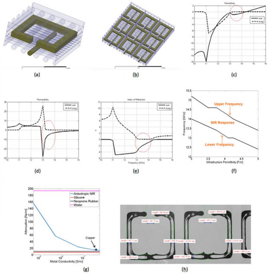
The design of the anisotropic negative index-of-refraction material went well. Incorporating direct ink-writing restrictions, we developed the split-ring resonator and dipole design shown in Figure 2(a,b). A single cell would consist of one split-ring resonator and one dipole made with silver-filled silicone, and lines of silicone. The cell measures 2.65 x 2.65 x 1.24 mm, with line widths about 250 μm, and would operate as a negative index-of-refraction from 13 to 14 GHz, as shown in Figure 2(c–e). Recognizing the nonideal nature of the direct ink-writing process, we examined effects of potential discrepancies between design and printed material.
From Figure 2(f,g), discrepancies in the permittivity of the substrate lead to a frequency shift of the negative index-of-refraction response. Low conductivity of the silver-filled epoxy leads to attenuation in the material that, if large enough, would prevent measurement, even for validation purposes.
To build the structure, we needed to be able to perform multi-material direct ink writing on a pattern with about 25 layers of split-ring resonators, dipoles, and all the intermediate layers. And we needed to develop a stretchable, printable, and conductive sample. We accomplished some of these goals. We established multi-material capability with direct ink writing using two nozzles. We created a procedure to register two nozzles to each other, and determined correct conditions for stop and start ink flow. We created pattern programs that included supports for the filament geometry for multiple layers and included multi-material printing capability. Finally, we patterned the negative index-of-refraction design out of nonconductive materials, as shown in Figure 2(h).
Developing flexible, printable conductive ink proved much more challenging than expected. We tried silicones loaded with conductive fillers (silver, carbon nano-fibers, and carbon nanotubes). Finally, after relaxing the stretchability requirement, we identified a silver ink (Alfa Aesar) that was conductive enough but needed to be modified for printability to flow through a 250-μm nozzle. After some development, we determined that the additional work required to print was too costly and we put this task on hold. As part of the process of developing the conductive ink, we developed the capability to measure conductivity of printed material at microwave frequencies. This capability still exists and could be taken advantage of in future work.
Measurement of anisotropic material can be challenging, especially when the samples are small. As such, many of the conventional methods, such as waveguide measurement and horn measurements, would not work. The use of a transmission electron microscopy cell was potentially possible, but historically, transmission electron microscopy cells are not used to characterize the response of a device under test to specific, controlled transmission electron microscopy waves, nor measure material properties.
Our solution was to develop a transmission electron microscopy cell (using simulation) with dimensions suitable to test the sizes of material we would eventually have available. We designed a structure that optimized radiation, but calibration proved challenging, because normal calibration methods did not work well. Given the significant challenge of finding a conductive ink, we redirected our resources away from this task until such time when we would have a material that we can test.
Three-Dimensional Isotropic Electromagnetic Metamaterial Based on an Underlying Mechanical Metamaterial Substrate
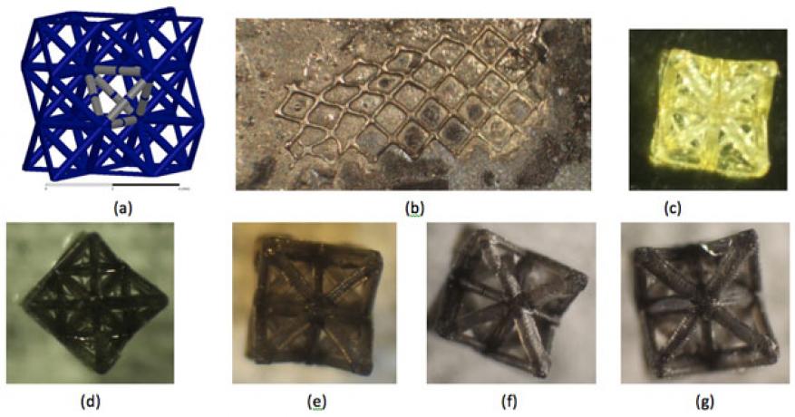
Our plan was to utilize the design heritage of the octet truss (mechanical metamaterial)5 to create a direct ink-writing metamaterial with an isotropic, negative permeability, shown in Figure 3(a), which shows the concept with split-ring resonators. To do this, we needed to be able to perform multi-material projection micro-stereolithography, with two very dissimilar materials (i.e., a metal and ceramic), or perform selective metallization.
We pursued selective plating using electroless nickel plating catalyzed with palladium nanoparticles. While electroless nickel plating has been performed on solid palladium, no one has accomplished it with palladium nanoparticles in resin. A quick test showed that electroless nickel plating is possible directly on the printed resin, as shown in Figure 3(b). Unfortunately we discovered that the photo-absorber in the resin interacts with the palladium chloride salts that we were initially using as our source of palladium. This reduced the salts but left the resin unable to cure and no measureable metal content, as shown in Figure 3(c–g). We began using palladium nano-particles instead of salts, but this pursuit was dropped with respect to the ceramic fabrication efforts.
Three-Dimensional Isotropic Electromagnetic Metamaterial Based on Ceramic Spheres
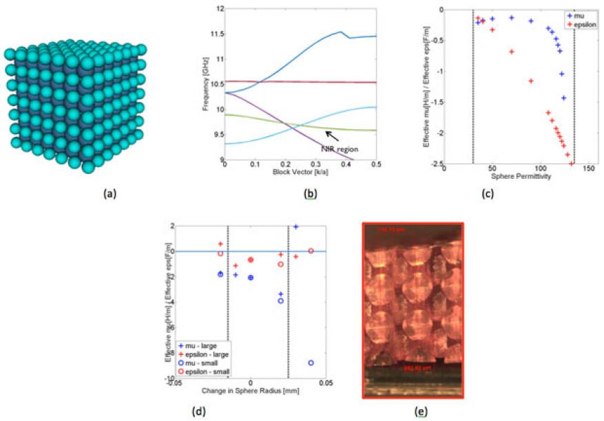
An alternate approach to achieve a three-dimensional isotropic electromagnetic metamaterial was to use two different-sized ceramic spheres, packed in a body-centered-cubic formation, shown in Figure 4(a). High dielectric permittivity spheres will exhibit both negative permittivity and permeability properties in certain frequency regimes based on sphere size and dielectric constant. Using a band gap calculation code from the Massachusetts Institute of Technology and the HFSS software for simulating three-dimensional full-wave electromagnetic fields, we determined the associated sphere sizes and permittivities needed, as shown in Figure 4(b–d). Then using projection micro-stereolithography, we demonstrated that printing this type of structure would be feasible, shown in Figure 4(e). Because the dielectric constant needed was quite high, we planned to use a barium strontium titanate and alumina nanoparticle mixture suspended in resin to create the spheres.
Optimized Mechanical Metamaterials to Produce User-Customizable Permittivities
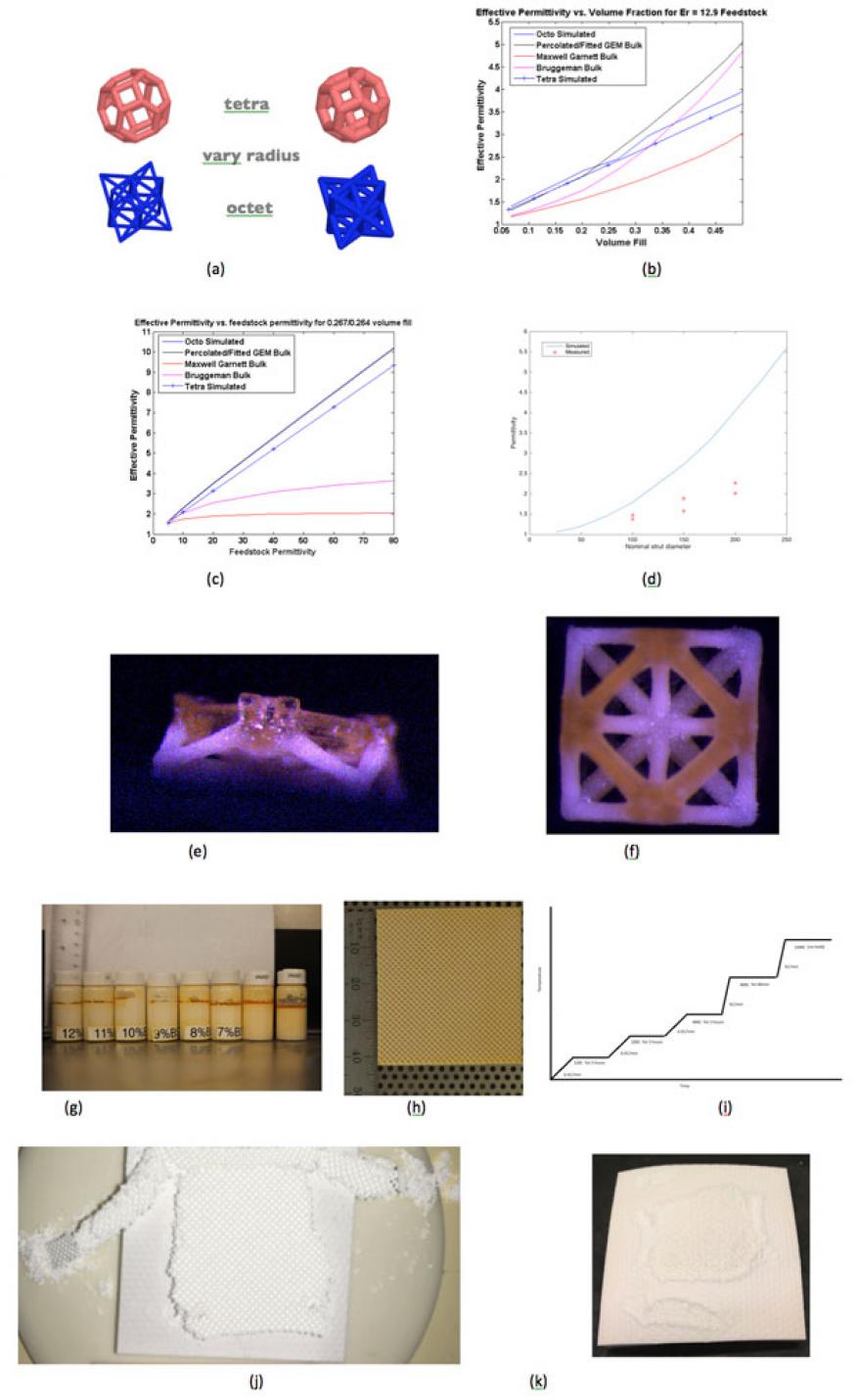
We wanted to demonstrate the potential for a made-to-order low-loss permittivity material, built on a variety of mechanical metamaterials that are chosen for desired mechanical properties. By varying feedstock radius (i.e., unit-cell fill factor) and feedstock permittivity (Figure 5), we can design for any permittivity, while maintaining the mechanical benefits of an optimized mechanical metamaterial. In addition, the performance is better than bulk mixing, while being strong and lightweight. Figure 5(b) shows how the permittivity varies as the volume fraction (or strut radius) increases. We see at low volume fractions (thinner struts), the simulated performance of the octet truss and tetrakaidekahedron (tetra) is much better than the most-common effective mixing equations predict. This result indicates that the tetra and octet should perform better than a homogeneous mixture at low mixing fractions. The reason is likely because of the structured nature of the material, which fits more closely to the percolated equations for electromagnetism and relativistic gravitation, at low mixing fractions. We see this same result as we vary the feedstock permittivity for a constant volume fraction, shown in Figure 5(c). This is exciting, because it will allow for much greater permittivities for small amounts of high-permittivity material.
To pursue these materials, we looked at ceramic nanoparticles in resin. After a de-bind and sinter step to remove the resin, we expected a strong, low-loss high dielectric-constant material. Our approach was to show the feasibility of using alumina, and a move to barium strontium titanate or a barium strontium titanate and alumina mixture that would yield a very high dielectric constant. Figure 5(d) shows a comparison of experimental measurements of alumina octet materials at low frequencies with simulation, where the solid line is expected response and the red crosses are the high and low measurement values. The simulation appears to over-estimate the dielectric constant. However, the parts did not seem to shrink as much as expected during de-bind and sinter, which may have led to struts that are not fully dense. In the simulations, the permittivity assigned to the alumina assumed a fully dense ceramic. The project concluded before we could determine the cause of the discrepancy.
In addition to alumina, we pursued resins filled with barium strontium titanate as well, but this turned out to be more difficult than expected. The stability of a resin over time is the main factor that determines if a part can be successfully printed and then sintered. The as-printed part must have a uniform particle distribution to remove the polymer and sinter the remaining barium strontium titanate particles into a solid part. Uneven particle concentration results in collapsed features and defects. Figure 5(e–f), show a part where the particle settled out during printing.
Through the use of ultraviolet–visible spectroscopy absorption measurements, settling studies shown in Figure 5(g), and trial and error, we reached the point where we successfully printed a part, Figure 5(h). Ultimately, however, we had trouble with the de-bind and sinter steps. The thermal burnout procedure is shown in Figure 5(i). The slow ramp and hold at 110, 220, and 400°C burns off the water, volatile organic compounds, and majority of the polymer, respectively. The higher temperatures ensure that the hydrocarbons and all traces of the polymer are gone. Damage occurred during the burn-out (de-bind), shown in Figure 5(j), possibly because of a buildup of gases. During the sinter step, the part seemed to have fused with the alumina substrate, shown in Figure 5(k). These problems are not insurmountable, but ultimately we ran out of time to pursue the issue.
Impact on Mission
Our research is important for the Laboratory's cyber security, space, and intelligence strategic focus area. It could lead to smaller microwave radar and communication components and systems, advanced microwave sensors, and greater design capabilities for any type of microwave system with user-specified materials. Creating a new class of metamaterials is also well aligned with Livermore's core competency in advanced materials and manufacturing. This project has increased collaboration between the Laboratory's electromagnetic and additive manufacturing groups, with potential applications of interest to a variety of external agencies.
Conclusion
We sought to create a new material class of electromagnetic and mechanical, negative index-of-refraction multifunctional metamaterials. Such class of materials will be the first three-dimensional isotropic negative-index materials in the microwave regime. This research could affect radar and communications system design, device miniaturization, advanced sensor design, and the practical realization of many negative-index devices that are currently just a theoretical or laboratory-based novelty. Examples of benefits are the potential for microwave invisibility, advanced antenna design with a significantly greater range of achievable sizes and form factors, and large lightweight components, such as 10-ft microwave lenses that weigh just a few pounds. This technology could also enable sensors in which stress and strain response is coupled to the electromagnetic response to maximize sensitivity or accuracy. For this study, we focused on multifunctional metamaterials that have interesting electromagnetic properties in the low gigahertz-frequency spectrum. We worked toward developing one-dimensional anisotropic electromagnetic metamaterials, three-dimensional isotropic electromagnetic metamaterials, and finally constructed materials designed for electromagnetic permittivity on mechanical metamaterial substrates. During the course of our research, we advanced the technology to bring electromagnetic metamaterials into practical use, as well as investigating multi-functionality of materials with respect to electromagnetic and mechanical properties.
References
- Liu, R., et al., “Negative index material composed of electric and magnetic resonators.” Appl. Phys. Lett. 90, 264504 (2007).
- Zhou, J., et. al., “Negative index materials using simple short wire pairs.” Phys. Rev. B 73, 041101 (2006).
- Koschny, Th., L. Zhang, and C. M. Soukoulis, “Isotropic three-dimensional left-handed metamaterials.” Phys. Rev. B, 71, 121103 (2005).
- Melik, R., et. al., “Metamaterial-based wireless strain sensors.” Appl. Phys. Lett. 95, 011106 (2009).
- Meissner, C., “Materials by design.” Sci. Tech. Rev. UCRL-TR-5200-12-3, 14 (2012).


