Monika Biener (16-FS-012)
Abstract
The goal of this project was to explore the feasibility of fabricating a thin (200 µm) low-density (<50 mg/cc) foam liner for deposition on the inside of a hollow cylinder by combining Electrophoretic Deposition (EPD) and Atomic Layer Deposition (ALD) templating. We successfully deposited smooth polystyrene (PS) bead films via EPD on flat electrodes. These films typically have a surface roughness value (Rq) of about two µm. Using well-defined drying conditions, we were able to avoid crack formation during the drying process. A uniform ALD coating several nanometers thick was then applied to the PS bead film, resulting in a composite foam layer (polystyrene/ALD coating). Complete removal of the sacrificial polystyrene template without formation of large cracks was achieved by plasma etching.
The transfer of the EPD process from the flat to a cylindrical electrode geometry was demonstrated on a stainless steel rod (7mm diameter). However, using a cylindrical gold electrode instead of the stainless steel cylinder resulted in an inhomogeneous EPD film with poor adhesion. These issues need to be addressed in future studies (possibly by surface pretreatment or roughening).
Background and Research Objectives
The goal of this study was to demonstrate the fabrication of ~200-µm-thick, sub-50 mg/cc porous coatings on the inside of a hollow cylinder. Such uniform low-density foam layers in a cylindrical geometry are directly applicable to a broader range of high-energy-density (HED) physics experiments (e.g., to suppress the high-Z wall motion as a source of drive asymmetry). The use of a foam liner inside the hohlraum could provide a critical degree of freedom for designs of the National Ignition Facility's Inertial Confinement Fusion (and high-energy-density) experimental platforms meant to increase the capsule absorbed energy.
The project objectives were to demonstrate that (1) Electrophoretic Deposition (EPD) can be used to fabricate a uniform film of densely packed sub-1µm-diameter polystyrene (PS) beads, (2) these PS-bead films can be used as sacrificial templates for atomic layer deposition (ALD), and (3) can be removed by chemical dissolution/thermal decomposition. We were able to reach most of these objectives for flat electrodes. The transfer to cylindrical electrodes was demonstrated on a stainless steel rod; however, delamination and inhomogeneity issues occurred when transferring the technique to a cylindrical gold electrode.
Scientific Approach and Accomplishments
To evaluate EPD process parameters and PS beads obtained from different vendors, we performed EPD test runs on flat electrodes (Au-sputtered Si flats). Parameters that were systematically varied included bead concentration, flow rate, pH, deposition current, and electrode pretreatment (piranha/plasma/ALD Al2O3). Beads with similar sizes were purchased from Spherotech and Polyscience (for details, see Table 1). We found that the quality of the EPD coating depends on the type of beads used in the experiments, and that only Spherotech beads (710-nm diameter, non-crosslinked and non-functionalized) reproducibly lead to flat deposits. All other bead types were either not depositing or showed a very inhomogeneous deposit.
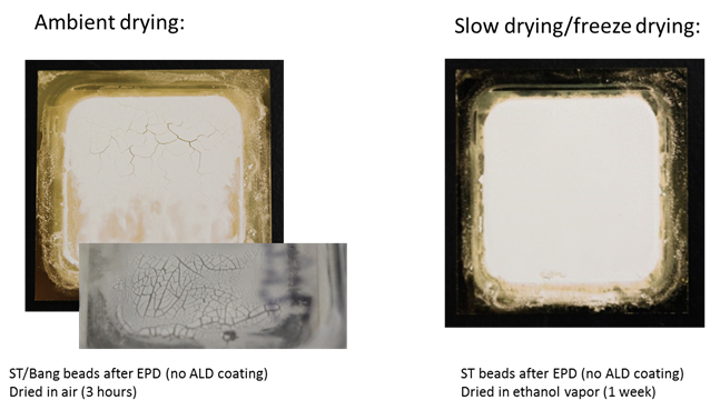
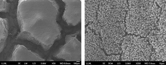
Ambient-air drying of the EPD deposit usually took approximately three hours and caused cracks to form on the deposited material. However, drying-induced crack formation could be prevented by slow drying in ambient ethanol vapor (i.e., in a membrane box with an ethanol-soaked wipe) over the period of one week (Figure 1). Alternatively, freeze-drying also led to crack-free samples.
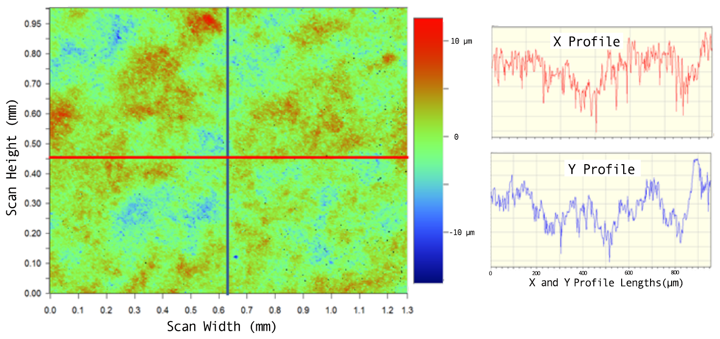
The surface-roughness parameter (R) was analyzed using whitelight interferometry. A scan taken from a flat sample (710 nm Spherotech beads, 140 µm thickness) is shown in Figure 2. The Rq (root mean squared) value for a ~1 mm2 scan of this sample is 2.26 µm, an acceptable surface-roughness value. Deposited films made using larger beads generally exhibited larger Rq values.
The thickness of the EPD layer was controlled by both deposition time and current (using the constant-current mode). As expected, the deposition rate increased with increasing current, but doubling of the current does not double the deposition rate (Figure 3). After an induction period of a few minutes, the EPD film thickness increased approximately linearly with time. The observation of an induction period during which the growth rate is zero (or very low) indicates that, initially, nucleation is rate limiting.
After drying, the EPD deposits were ALD coated with Al2O3. We used the well-established trimethyl-aluminum (AlMe3/H2O) ALD process in a warm-wall reactor (wall and stage temperature of 90 °C). Long exposure and purge times (300 seconds each) were used to ensure uniform coatings throughout the porous material. The resulting increase in the ALD film thickness was strongly dependent on the bead type, as indicated by the different equivalent ALD coating thicknesses shown in Table 1. All samples shown in the table were coated using the same ALD parameters (15 cycles) targeting a thickness of three nanometers.
The large variation of the ALD growth rate observed for different beads (Figure 4), from 0.3 nm/cycle to 0.7 nm/cycle, indicates deviations from the ideal layer-by-layer ALD behavior. Indeed, ALD deposition within the polymer increases the apparent deposition rate.
The ALD deposition behavior also affects the template-removal step. We tested several different approaches to removing the polymer template, including dissolution of the polymer in solvents (i.e., xylene) and burnout by either heating in air (two hours at 450 °C) or by an air-plasma treatment (RF plasma). The success of the template-removal process was measured by material weight loss. In general, we observed that the treatment with solvents did not remove the template. By contrast, heating in air did completely remove the PS templates, but induced the formation of large cracks (or shrinkage, as in the case of non-supported ALD-coated polystyrene bulk samples).
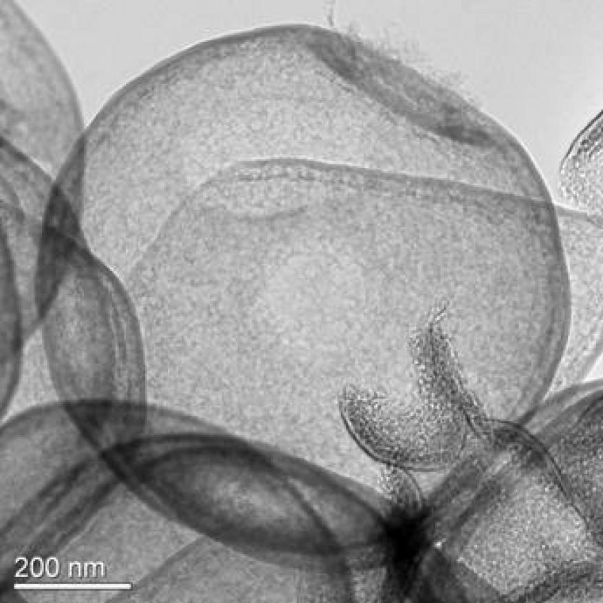
Samples coated with only thin ALD films and made from polystyrene templates that showed high ALD growth rates (indicating infiltration of the ALD precursor in the polymer matrix and subsurface ALD deposition) were prone to crack formation. High-magnification scanning electron microscopy images (Figure 5) revealed that the high-temperature-air treatment did not only induce macroscopic defects (such as the cracks discussed above), but induced rupturing of individual ALD film shells due to the high pressure that builds up in the shells. The room-temperature air-plasma treatment also removed the polystyrene template, albeit at much lower rates, and drastically reduced the size of the cracks formed in the ALD templated EPD layer (from hundreds of microns for air burnout to less than 10 µm by comparison; see Figure 5). Complete template removal was achieved for thin ALD coatings (15 Al2O3 ALD cycles) and 48 hours of exposure to the air plasma. In the case of the air-plasma treatment, it was observed that the etching of the PS spheres started in the vicinity of cracks and progressed from there into crack-free regions of the samples. This indicates that small ALD coating defects formed during crack formation are critical for the air plasma template removal.
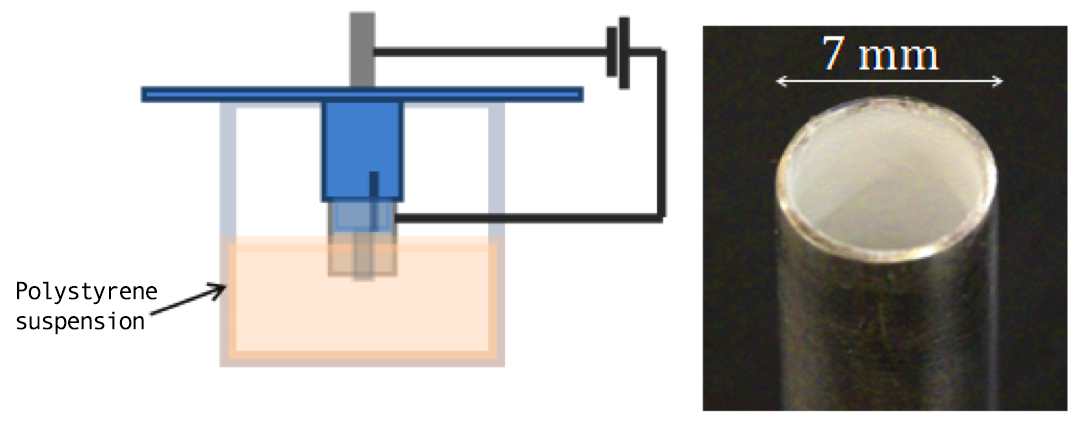
Finally, we demonstrated that the EPD technology can be transferred from the flat test geometry to the cylindrical geometry needed for the hohlraum liner application. In order to perform EPD in this geometry, we designed and 3D-printed a new sample/counter electrode holder. In contrast to the plane-parallel configuration for the flat-test geometry, the counter electrode was placed on the center of the cylinder. To avoid thicker coatings at the edges of the cylinder due to local field enhancement, the counter electrode needs to be retracted inside the cylinder. Using this geometry, we deposited uniform films on the inside of a stainless steel cylinder (Figure 6).
Similar experiments on gold cylinders resulted in non-uniform coatings and poor adhesion of the deposit to the surface. We attribute this to nucleation-limited growth on the gold surface. Future experiments will explore if the nucleation can be facilitated by surface roughening or coating with a hydrophilic metal-oxide film such as ALD Al2O3.
Impact on Mission
Our approach of creating ideal conformal coatings using novel techniques supports Lawrence Livermore National Laboratory's core competency in advanced materials and manufacturing. The EPD coating capability developed during this project greatly expands the fabrication parameter space for low- to mid-Z hohlraum liners to control deleterious wall motion. It will enable cost-efficient integration of tailored low-density foam liners into hohlraums used in Inertial Confinement Fusion and other types of HED physics experiments relevant to the National Ignition Facility and other Laboratory research efforts. A central challenge in hohlraum design is the need to suppress the high-Z wall motion as a source of drive asymmetry. The use of tailored foam liners could provide an important degree of freedom for designs of Inertial Confinement Fusion (and HED) experimental platforms meant to increase the capsule absorbed energy.
Conclusion
Our work demonstrated that it is possible to make 200-µm-thick foam layers with a density of less than 50mg/cc using the EDP/ALD templating approach. The transfer of the EPD process from planar test geometry to the desired cylindrical geometry was demonstrated but it needs further improvement. Specifically, adhesion and homogeneity issues need to be addressed when using a cylindrical gold electrode. We propose to establish an in-house capability to synthesize tailored polystyrene beads that may improve the reproducibility and quality of the EPD layer.
Publications and Presentations
Biener, M. M. 2017. "Coating Hollow 3D Objects with Uniform Low-Density Films by Combining EPD and ALD." Las Vegas, NV,12—16 March, 2017. LLNL-PRES-725737.


