Andrea Schmidt (16-FS-035)
Abstract
High-power impulse magnetron sputtering (HiPIMS) is a new type of magnetron sputtering with established uses in industry, in which the sputtered material emerges from the target ionized. Ionization of the depositing atoms, when coupled with a substrate bias, enables a new level of control over the energetics of the depositing species and enables nonplanar substrates to be coated more uniformly. Negative, or bias, voltage applied to a substrate influences the energy and direction of motion of the positively charged particles that hit the substrate. We investigated the feasibility of this new sputtering process for use in optical films, as well as created a modeling capability that can be used to understand the conditions needed to increase sputtering rate. Our successful study established a new HiPIMS capability at Lawrence Livermore. We used the technique to deposit four film material systems of copper, aluminum, platinum, and platinum–iridium, and also deposited films of these materials without an HiPIMS technique for reference purposes. We characterized the films for thickness and deposition rate, stress, chemical composition, and surface morphology. We observed that for all the material systems except platinum–iridium, the sputtering technique increases the compressive stress. For copper this was ideal in that it transformed a tensile film into one with near-zero stress. For platinum–iridium, it also lowered the stress (at low bias voltages), and there is some qualitative evidence of adhesion promotion of the platinum–iridium during a lift-off lithography process performed when it was deposited on a patterned wafer. There is also some data suggesting that HiPIMS altered the preferred orientation of the copper films. Energy dispersive spectroscopy suggested that argon incorporation was generally low, but no particular improvement was observed with HiPIMS. We did, however, observe a significant decrease in the deposition rate. Overall, the data suggests that our new sputtering technique does affect film stress and the microstructure, but more work is needed in terms of optimization for particular coating applications.
Background and Research Objectives
A relatively new technique, HiPIMS creates ionized material as it emerges from the target. Ionization of the depositing atoms, especially when coupled with a substrate bias, enables a new level of control over the energetics of the depositing species. This added level of control over the depositing species energetics should enable the film stress and microstructure to be controlled more readily than with conventional magnetron sputtering or even variants of it such as unbalanced magnetron sputtering. Therefore, lower-stress and higher-density films become possible in material systems where this has been hard to achieve previously. It also should enable nonplanar substrates to be coated with less concern of obtaining nonuniform and lower-density films because of shadowing effects, which is a problem in conventional magnetron sputtering. Livermore's National Ignition Facility, for example, is interested in using this new coating technique to advance their optics and targets capabilities. Here we describe our effort to establish the first HiPIMS capability at the Laboratory and initial results on the synthesis and characterization of films using this technique.
Scientific Approach and Accomplishments
We obtained a low-cost HiPIMS pulsar from Starfire Industries in Champaign, Illinois, and it was connected to a conventional direct-current magnetron sputtering power supply. This main supply provided voltage and power for the Starfire pulsar, which then performs a time-compression of the current coming from the main supply, imposing a high current (~100–200 A) on the magnetron target.
The experimental conditions used to synthesize films via HiPIMS are shown in Table 1. Peak currents were calculated from oscilloscope traces for each of the four material systems. It is evident that relatively high peak currents (a relative measure of the intensity of the HiPIMS process and the ionization of the sputtered depositing species) are achieved with copper and aluminum. Less peak current was observed with the platinum and platinum–iridium targets, possibly because of their resistivity.
Table 1. Experimental conditions used to synthesize films via high-power impulse magnetron sputtering.
| Material | Voltage on source (V) | Power on source (W) | Argon pressure (mTorr) | Sputtering repetition rate (Hz) | Sputtering pulse width (ms) | Sputtering peak current (A) |
| Copper | 465 | 200 | 4.6 | 80 | 60 | 278 |
| Aluminum | 765 | 100 | 3.7 | 40 | 50 | 245 |
| Platinum | 995 | 125 | 6.0 | 100 | 50 | 45 |
| Platinum–Iridium (60/40%) | 780 | 100 | 4.6 | 100 | 65 | 41 |
Film thicknesses were characterized by a Veeco Dektak 150 Profilometer. Film stress was measured on a Tohu Technology FLX 2320-S Thin Film Stress Measurement System. A scanning electron microscope, focused ion beam, and energy dispersive spectroscopy system was used for characterization. Scanning electron microscopy was used for imaging—the images shown here were taken at approximately 65,000-times magnification or higher. Energy dispersive spectroscopy at 15 keV on the same tool was used for chemical analysis, including argon incorporation estimates, and focused ion beam (also on the same tool) was used to create a section for imaging.
Copper, Aluminum, and Platinum
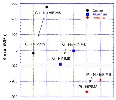
When we used HiPIMS to deposit films in copper, aluminum, and platinum, we found that the film stress became more compressive (Figure 1). For copper, which had a +278 MPa tensile stress for conventional magnetron sputtering, the HiPIMS process brought the film to near zero stress of −19 MPa compressive. It is significant that HiPIMS could render a near-zero stress copper film. With optimization of the bias voltage and other parameters, it is likely we could further lower the copper film stress using HiPIMS. Aluminum and platinum films, which were already compressively stressed with conventional magnetron sputtering, became more compressively stressed with HiPIMS deposition (Figure 1, Table 2). It should be noted the platinum films showed some delamination, so the stress values prior to delamination could have been higher.
Table 2. Results for the thickness and stress of copper, aluminum, and platinum films deposited with and without high-power impulse magnetron sputtering (HiPIMS).
| Sample ID | Approximate film thickness (μm) | Stress 1 at 0° (MPa) | Stress 2 at 90° (MPa) | Mean stress (MPa) | Description/comments |
| 4-16-0929 | 0.14 | −16 | −22 | −19 | Copper HiPIMS with −55 V bias |
| 4-16-0928 | 1.80 | +278 | +279 | +278 | Copper with no HiPIMS or bias. |
| 4-16-0924 | 0.15 | −88 | −88 | −88 | Aluminum HiPIMS with −55 V bias |
| 4-16-0927 | 0.38 | −6 | −2 | −4 | Aluminum with no HiPIMS or bias |
| 4-16-0829 | 1.38 | −173 | −171 | −172 | Platinum with no HiPIMS or bias |
| 4-16-0830 | 0.74 | −232 | −302 | −267 | Platinum HiPIMS with about −60 V bias |
Table 2 also lists film thickness. For the copper films, the same power (200-W average) and deposition times (1/2 hour) were used for both the HiPIMS and non-HiPIMS film deposition runs. Note the dramatic difference in film thickness: the film with HiPIMS is approximately 0.14-μm thick, whereas the one without HiPIMS is about 1.8-μm thick, suggesting a drop of over 90% in the deposition rate for this system under these particular conditions. The main acknowledged drawback with HiPIMS is a drop in deposition rate, but this level of a drop is still very high by most standards. It is indicative that we have obtained a high degree of metal ionization, and also that the magnetron used has a relatively balanced magnetic structure. We confirmed the approximately 0.14-μm-thick value with a focused ion beam cross-section imaged in a scanning electron microscope. We are hoping to address and improve the deposition rate with kinetic magnetron plasma modeling under future projects, including a DOE High Performance Computing for Manufacturing collaboration with the Applied Materials manufacturing company in Santa Clara, California.
For the aluminum films, which were created with about 1/2 hour deposition times and 100-W (average) power for both the HiPIMS and non-HiPIMS runs, we see a significant drop in the deposition rate. It is, however, not as dramatic: 0.38 μm for non-HiPIMS aluminum films to 0.15 μm for HiPIMS aluminum films. For platinum, we did not utilize the same power levels for the HiPIMS and non-HiPIMS samples, making a quantitative deposition rate comparison less accurate. Assuming the deposition rate is linear in power, the experiments indicate that the platinum deposition rate is about two to three times lower with HiPIMS.
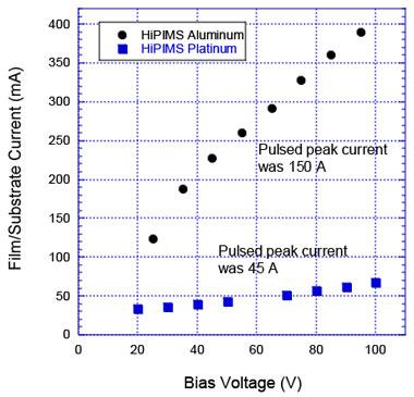
We also measured the ion current on the substrate as a function of substrate bias voltage for both aluminum and platinum under a particular set of conditions (Figure 2). Considerably more ion current is obtained with the aluminum than the platinum with HiPIMS, an expected result because aluminum has a much higher peak discharge current (150 A) than platinum (45 A). The absolute values of measured ion currents have some error because of secondary electron emission from ion impact on the film.
Table 3. Argon incorporation values as measured by energy dispersive spectroscopy for copper, aluminum, and platinum high-power impulse magnetron sputtering (HiPIMS).
| Sample ID | Film | HiPIMS? | Bias voltage | Argon (atomic %) | Description/ comments |
| 4-16-0929 | Copper | Yes | −55 V | 0.32% | |
| 4-16-0928 | Copper | No | No | 0.09% | |
| 4-16-0924 | Aluminum | Yes | −55 V | 0.90% | |
| 4-16-0927 | Aluminum | No | No | 0.41% | |
| 4-16-0829 | Platinum | No | No | 0.85% | |
| 4-16-0830 | Platinum | Yes | −60 V | 0.0% | Delamination |
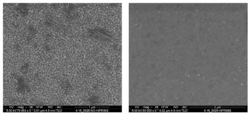
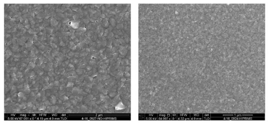
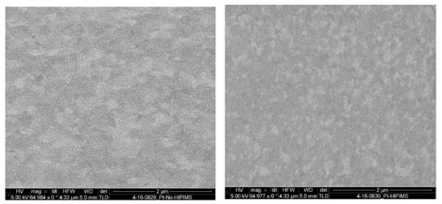
We also examined the surface morphology via scanning electron microscopy with and without HiPIMS at high magnifications (Figures 3–5). One can see clear differences in grain sizes and structure between the two types of film. These structural differences may have implications for leak tightness, but we did not have time to test the films accordingly in this feasibility study.
During this feasibility study, we also began work on HiPIMS films using a platinum–iridium target. Platinum–iridium (and the corresponding oxide) are of interest for biomedical implant devices, but there is very little information on HiPIMS in these materials in the literature. It is a challenging system to deposit, but our results with this material are new and of potential interest to the scientific community. The peak currents we obtained with this much thinner platinum–iridium target were comparable to those obtained with platinum and quite different from the measured currents in copper and aluminum. The materials used may have more of an impact on the current than the target thickness. This can be explained by the two effects that greatly affect plasma composition and degree of ionization, namely the sputtering yield affecting plasma composition, and the yield of secondary electrons, affecting ionization. Secondary electrons are accelerated in the target’s electric sheath, gaining high energy (about 80% of the applied voltage), and enabling them to produce many new electron–ion pairs.
Unlike what we observed for the copper, aluminum, and platinum, the platinum–iridium alloy films demonstrated a modest decrease in the compressive stress with HiPIMS. The compressive stress was −1,378 MPa without HiPIMS and was −1,008 to −1,127 MPa with HiPIMS at a variety of biases from −5 to −60 V. As the HiPIMS bias was taken higher, to −85 to −90 V, the compressive stress increased again to −1,432 to −1,475 MPa. It should be noted that this alloy film has much higher compressive stress overall than the copper, aluminum, and platinum films, so it may be the case that HiPIMS can reduce the compressive stress when stress values are relatively high. Stress evolution as a function of bias is generally nonlinear and even non-monotonic, as seen in this system. This is because initial ion bombardment can push ions into small interstitial spaces on the surface, while subsequent higher-energy ions can create collision cascades that relax the material on the surface and reduce the stress. Another effect is the modification of argon incorporation, partially dictated by the surface temperature, which varies with bias. The complicated relationship between bias and film stress should be further explored for each system and optimized for the specific application.
The deposition rate of the platinum–iridium film with no HiPIMS was measured to be 21 nm/min. With HiPIMS, the deposition rate decreased to 8 to 14 nm/min, depending on the bias. The high bias (which was not useful for decreasing stress) had the lowest deposition rates, while the lower biases shown to decrease compressive stress were roughly 12 to 14 nm/min. As noted before, platinum–iridium films are of interest for applications involving biomedical implant devices. Earlier this year, we sputtered platinum–iridium alloy films on patterned substrates and a liftoff process was applied. All of the features lifted off, which is undesirable. As part of this project, we also deposited platinum–iridium films on patterned substrates using HiPIMS (−25 V bias). Although many of the features still lifted off, the wafer was an improvement over the initial effort earlier in the year. This suggests that the HiPIMS platinum–iridium exhibited better adhesion in the lift-off process, a lithography process that will be needed if the platinum–iridium is to be used in biomedical impant devices in the future.
Impact on Mission
By demonstrating the feasibility of controlling film properties such as density and stress through ionization of deposited atoms using an HiPIMS system, coupled with substrate bias, this study aligns with the Laboratory's core competency in advanced materials and manufacturing. The strategic focus area of inertial fusion science and technology is supported by the proposed system's potential impact on laser-fusion target fabrication capabilities.
Conclusion
With this feasibility study we successfully established a new HiPIMS capability at LLNL. We used this capability to deposit four film material systems with HiPIMS—namely copper, aluminum, platinum, and platinum–iridium. We also deposited films of these materials without HiPIMS for reference purposes. We characterized the films for thickness and deposition rate, stress, chemical composition, and surface morphology. We observed that for all the material systems, except platinum–iridium, HiPIMS increases the compressive stress. For copper this was ideal in that it transformed a tensile film into one with near-zero stress. For platinum–iridium it also lowered the stress (at low bias voltages), and there is some qualitative evidence of adhesion promotion of the platinum–iridium during a lift-off lithography process performed when it was deposited on a patterned wafer. Energy dispersive spectroscopy suggested that argon incorporation was generally low with both techniques, but no particular improvement was observed with HiPIMS. We did observe a significant decrease in the deposition rate with HiPIMS, which is typical for this technique. Overall, the data suggests that HiPIMS does affect film stress and the microstructure, but much more work is needed in terms of optimization for particular coating applications.
We will be leading a new Livermore-based DOE High Performance Computing for Manufacturing collaboration with the Applied Materials manufacturing company. It will have a focus on modeling efforts to understand HiPIMS in the hopes of increasing the deposition rate, and our work in this project on deposition rate effects will be valuable for that effort. A new LDRD exploratory research project in FY17 will work toward understanding and optimizing HiPIMS for films with an eye on future National Ignition Facility target applications, and the knowledge and tools obtained in this feasibility study will be leveraged so that the new project will be more productive (especially in the first year). It should be noted that a topic deserving further attention is the potential ability of HiPIMS to coat nonplanar surfaces, which is of interest for laser targets and other applications.


