Selim Elhadj (15-ERD-057)
Project Description
Transparent conductive electrodes fulfill essential functions in optical-electronics applications, including light-harvesting solar cells, display panel controls, and energy-efficient windows with selective light filtering. Compact high-repetition-rate lasers use Pockels cells (a type of wave plate) that also require transparent conductive electrodes. In addition, these electrodes are found in spatial light filters such as those used for damage management in high-fluence lasers and in systems being explored for rapid additive manufacturing. In these demanding applications, transparent conductive electrodes are often limited by optical damage. We plan to develop processes, along with materials used in the electrodes, that can withstand irradiation from high-power lasers. Optoelectronics film susceptibility to optical damage can limit laser power and add steep design constraints to a laser and its size. We will determine optical failure modes and produce high-damage-threshold transparent conductive electrodes with fast electrical transport. This will be achieved by probing next-generation wide-gap semiconductors prepared using conventional and new thin-film fabrication techniques coupled to enhanced laser annealing.
We expect to identify optical failure modes and optimize fabrication of transparent conductive electrodes on robust substrates using conventional and new film-synthesis approaches that include enhanced laser annealing. We will assess films with respect to the optical damage threshold and conductivity trade-off. This knowledge and capability can support development of high-power lasers, such as repetition-rated, high-average-power, and small form-factor lasers being deployed in scientific exploration. Computational capability will be established that simulates laser sintering of nanometer-scale particles, which minimizes film defects and can impact additive manufacturing. In addition, we will develop the capability for doped nanoparticle-synthesis building blocks.
Mission Relevance
This work can enhance the performance of high-power lasers used in core missions throughout the Laboratory, including lasers for inertial fusion energy, and potentially new laser systems for parallel, fast, laser-based additive manufacturing technologies in support of Livermore's core competencies in lasers and optical science and technology and advanced materials and manufacturing. Extending our understanding of transparent conductive electrodes synthesis and optical failure modes may also support the strategic focus area in cyber security, space, and intelligence for protection of systems that rely on high-performance optoelectronics. Finally, transparent conductive electrode improvements can extend to multiple related applications involving energy production such as solar-cell transparent electrodes and conservation with selective light filters, relevant to the strategic focus in energy and climate security.
FY16 Accomplishments and Results
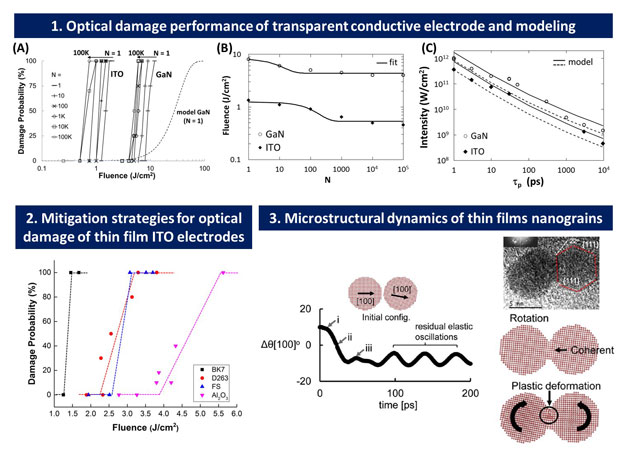
In FY16 we (1) determined optical failure mechanisms under pulsed laser exposure of transparent conductive oxides: indium tin oxide and aluminum zinc oxide, as well as periodic table groups three to five gallium nitride and silicon carbide materials; (2) identified single- and multiple-exposure failure modes stemming from free-carrier absorption and accumulated thermal and mechanical stress for indium tin oxide thin films, and to precursors for gallium nitride; (3) established that damage occurs in gallium nitride at interfaces, which correlates to carbon–oxygen complex impurities with a strong-ultraviolet photoluminescence signal; (4) demonstrated a diagnostic to detect optically weak gallium nitride; (5) demonstrated lifetime performance improvement of about tenfold over existing oxide film transparent electrodes with periodic table groups three to five materials (see figure); (6) conducted transmission electron microscopy experiments that revealed grain boundary dynamics under simulated laser heating conditions; (7) achieved increases in damage threshold by laser conditioning of gallium nitride and reducing the number of film interfaces; and (8) commissioned an in-house sputter unit to test means for improving optical strength of oxide films.
Publications and Presentations
- Lange, A. P., et al., "Dislocation mediated alignment during metal nanoparticle coalescence." Acta Mater. 120, 364 (2016). LLNL-JRNL-695366. http://dx.doi.org/10.1016/j.actamat.2016.08.061
- Yoo, J. H., et al., "Laser damage mechanisms in conductive widegap semiconductor films." Optic. Express 24(16), 17616 (2016). LLNL-JRNL-694293.


