Anna Hiszpanski (16-LW-041)
Abstract
Optical metamaterials are composites engineered to have unique optical properties not found in nature, thereby enabling their use in optical applications previously considered to be impossible. However, because the structure of optical metamaterials must be subwavelength in size, metamaterials operating at visible wavelengths require features that are 100 nm or smaller. Such small resolutions typically require top-down lithographic fabrication techniques that are not easily scaled to areas that are several square centimeters in size. We developed a new fabrication technique to make three-dimensional optical metamaterials that are functional at visible wavelengths and scalable to cover centimeter-square areas. Our new technique employed directed assembly of block copolymer systems (which are composed of two or more covalently linked and chemically distinct polymeric units or blocks) to form nanometer-scale structures with the required periodicity. Our structures are smaller in size (less than 100 nm) and cover a larger area than what has been achieved with traditional nanofabrication techniques. To guide our experimental efforts, we developed an algorithm to calculate the expected optical properties (specifically, the index of refraction) of such metamaterials. In so doing, we were able to achieve surprisingly large changes in optical properties with only small changes in the metamaterials’ structures. We also found that the ordered metal nanowire meshes produced by our scalable metamaterial-fabrication technique may act as transparent electrodes, which are needed in electrical displays and solar cells. We explored the feasibility of using ordered metal nanowires meshes for this application and developed design guidelines to aide our experimental efforts.
Background and Research Objectives
The field of optics was long limited by the optical properties of materials found in nature, but the rise of metamaterials, which are designed composites with subwavelength periodic structures, over the last two decades has revolutionized what scientists believe is possible in the optics field. The optical properties of metamaterials are determined by their constituent materials and the details of their patterned subwavelength structures. The optical properties of metamaterials can be tuned to values beyond those found in nature by making simple changes in the geometry of their subwavelength structures (i.e., their dimensions) or by selection of their constituent materials. For example, all naturally occurring materials have a positive index of refraction, but metamaterials can be designed to have a negative index of refraction, which can enable the production of structures previously considered impossible, for use in applications such as cloaking devices and perfect lenses (Shalaev 2007; Smith et al. 2000; Veselago 1968). Since the first demonstrations of such “cloaking” negative-index metamaterials at microwave wavelengths (Schurig et al. 2006; Smith et al. 2000), much effort has been dedicated to translating these results to visible wavelengths.
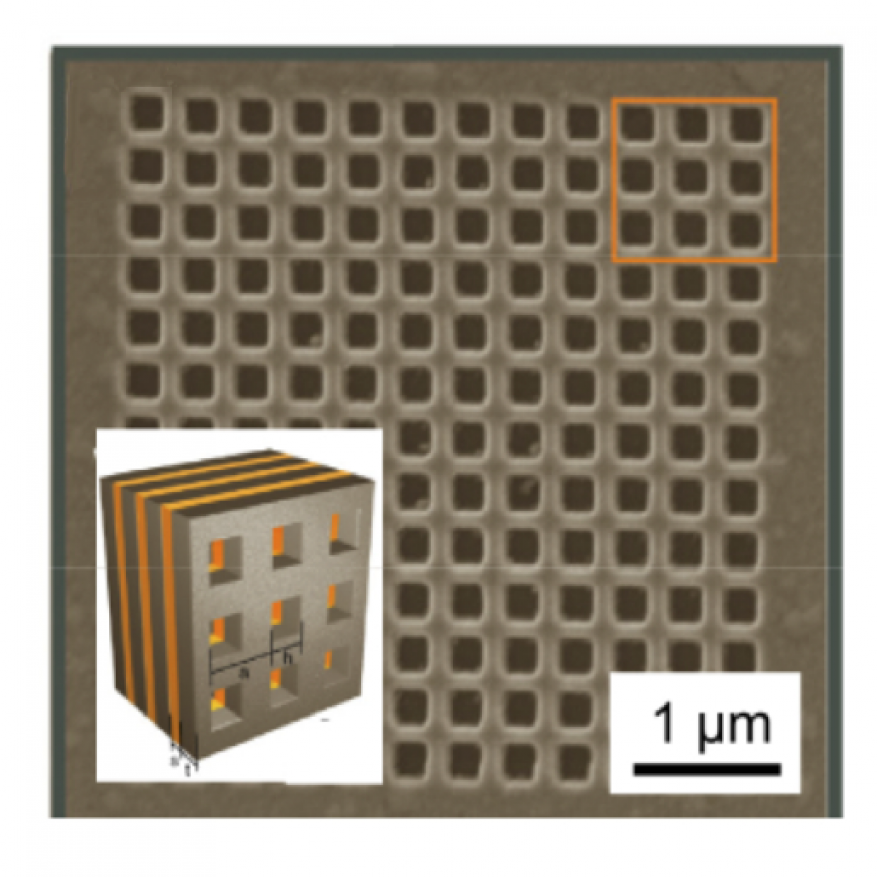
To this end, it was found that “fishnet structures” consisting of alternating metal and dielectric layers with a mesh-type of lattice structure with features on the order of 100 nm (Figure 1) can attain negative indices of refraction at visible wavelengths. However, fabricating such subwavelength structures is challenging, typically requiring traditional nanofabrication techniques (i.e., electron-beam, focused-ion-beam, interference, and nanoimprint lithographies) that are not scalable to large areas or depths, which limits both the lateral size and dimensions of potential structures (Soukoulis and Wegener 2011). Thus, to realize the applications of optical metamaterials beyond the lab scale, novel fabrication approaches that provide structural control on the sub-100 nm length scale and over areas several cubic centimeters are necessary.
The goals of this project were (1) to develop a new block-copolymer- (BCP-) derived method to fabricate fishnet optical metamaterials with <100-nm features over large areas and (2) to model the expected index of refraction of our targeted structures to understand how changes in the dimensions and thickness of optical metamaterials affect the index of refraction. We have achieved both these objectives for the project; we plan to submit a paper on Objective 1 and have published a paper on Objective 2. Furthermore, in the course of fabricating our fishnet optical metamaterials, we discovered that the metal layer of the fishnet structure by itself has significant potential use as a transparent electrode material. To evaluate the potential of our BCP-derived metal nanowire meshes for transparent electrode applications became our additional Objective 3. Transparent electrode materials are necessary in electrical devices that either absorb light (i.e., solar cells and photodetectors) or emit light (i.e., electronic displays). A replacement transparent-electrode material for indium tin oxide (ITO), the most widely used transparent electrode on the market, is highly sought after because indium is a critical material with a limited supply. We published an additional paper on this potential application of our structures and have submitted a patent application as well.
Scientific Approach and Accomplishments
Objective 1: Develop a Scalable Approach to Make Fishnet Metamaterials Over Large Areas
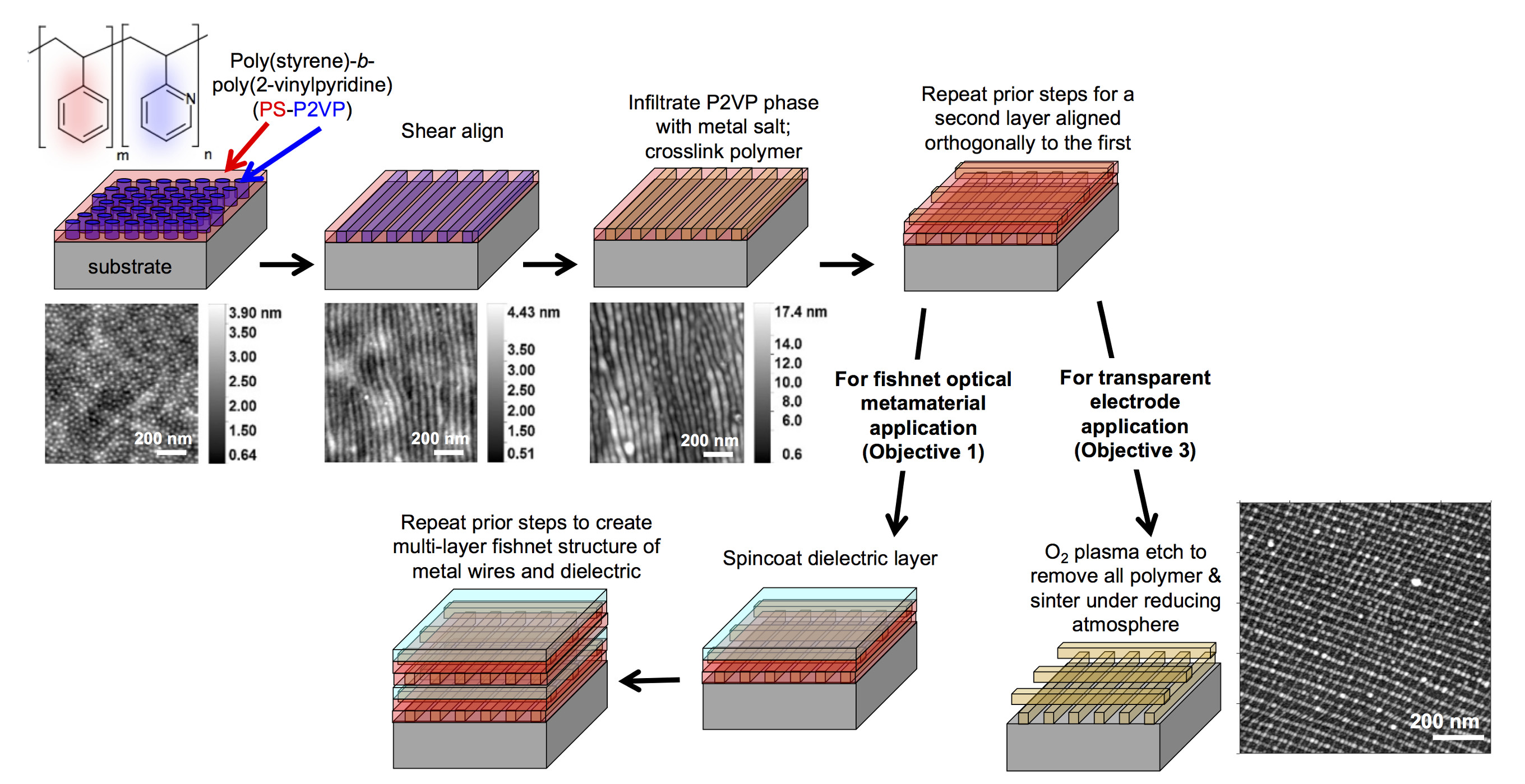
We proposed a novel fabrication scheme to make fishnet metamaterials using BCPs, as depicted in Figure 2.
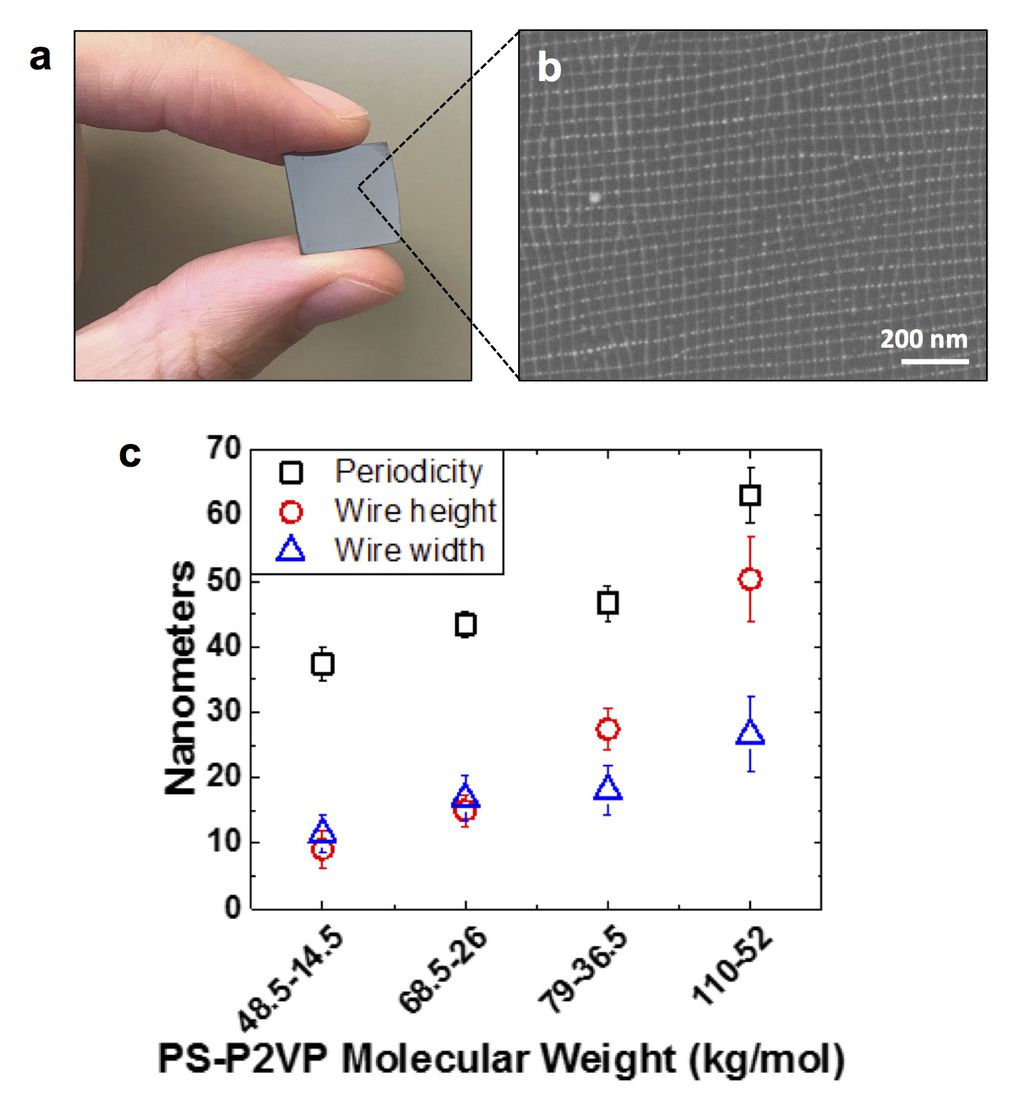
BCPs consist of two chemically dissimilar but covalently linked polymers (or "blocks") that microphase separately to form one of several patterns (such as spheres, cylinders, or lamellae) with 10–100 nm features (Bai and Ross 2016). While BCPs do not naturally form the kind of long-range straight-line patterns needed to create a fishnet pattern, it was previously demonstrated that applying shear force to BCPs can cause them to rearrange into line patterns oriented in the direction of applied shear force with long-range ordering (Angelescu et al. 2004; Kim et al. 2014). Repeating this process in two layers creates a fishnet-type mesh, and stacking multiple such layers atop one another enables the construction of the targeted fishnet metamaterial structure. As proposed, we successfully leveraged this technique to create subwavelength metal lattices (see Figures 3a and 3b) over areas of several square centimeters that can be layered atop one another with dielectric layers in between to produce the fishnet architecture.
We chose to use the commercially available BCP poly(styrene)-b-poly(2-vinylpyridine) (PS-P2VP) since the P2VP phase complexes with metal salts (Chai et al. 2007), thereby providing a means of directly creating metal nanowires from the shear-aligned BCP rearranged into lines. We discovered that the dimensions and periodicity of the nanowire arrays produced from BCPs can be easily tuned by the degree of its polymerization (i.e., molecular weight), as shown in Figure 3c. Furthermore, the type of metal nanowires formed can be varied simply by selection of the metal salt (Chai et al. 2007). We found that the quality of shear alignment and resulting nanowires depends on several factors, including the BCP's molecular weight, the thickness of the film, and the shearing time; we optimized these conditions to attain high-quality metal nanowire meshes with few defects over approximately 4-cm2 areas with tunable <100-nm dimensions and geometry. Furthermore, we designed and developed a pneumatic-based shear-aligning system that is capable of handling 4-in. wafers, thereby allowing us to scale to yet larger areas.
Objective 2: Evaluate the Optical Properties of Metamaterials
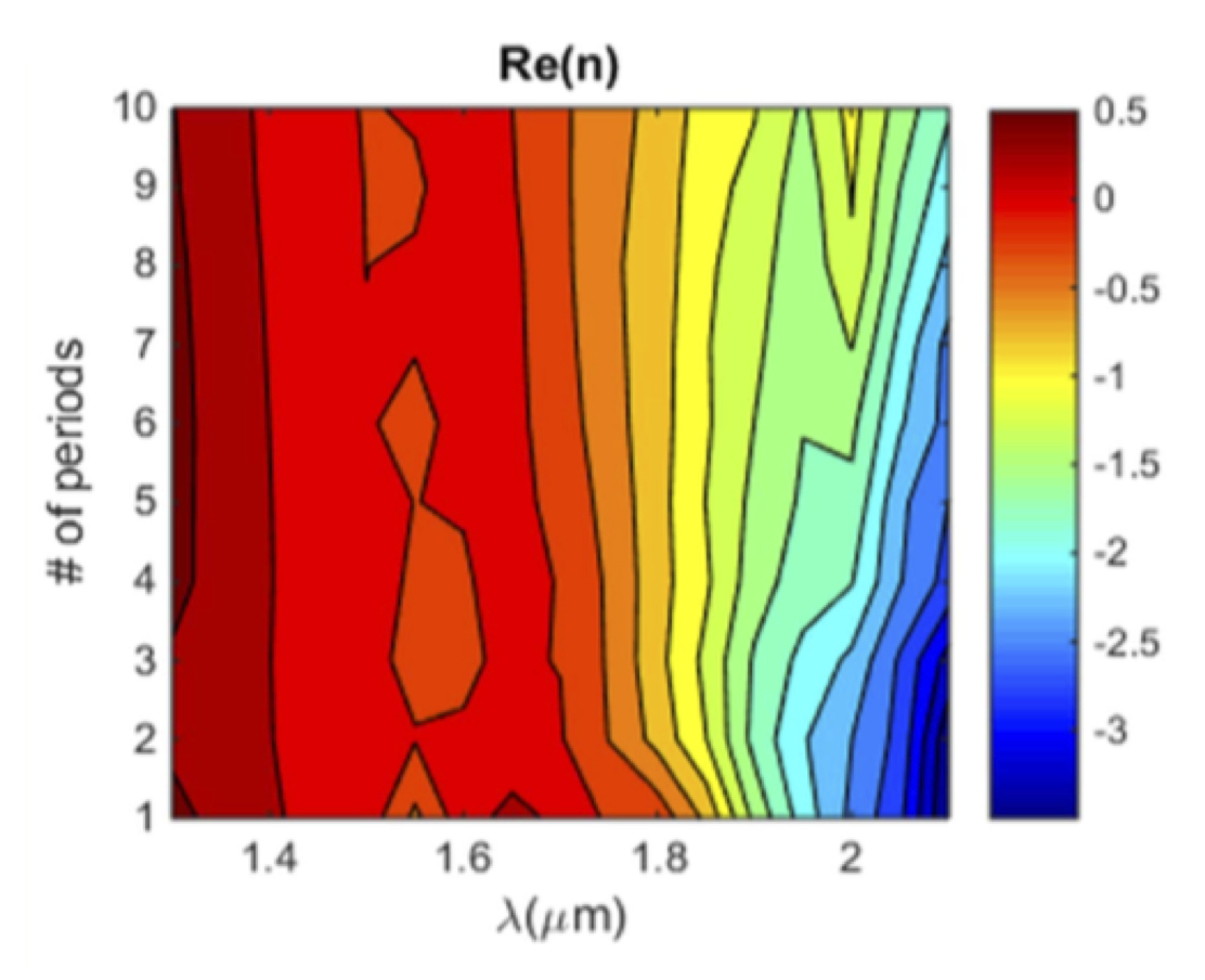
Given that (1) our BCP-derived method of creating fishnet metamaterials provides tunability over the dimensions of the structure and that (2) the dimensions we can access are approximately one order of magnitude smaller than those previously explored, we next performed simulations to understand how the optical properties of these structures change as a function of their subwavelength dimensions. The techniques reported in the literature to calculate metamaterials’ effective index of refraction treat the metamaterials as “black boxes.” However, we found that these techniques are not robust as they yield erroneous and unrealistic indices of refraction if the right constraints are not chosen; the right constraints are not necessarily apparent a priori. Thus, rather than treat the metamaterial as a black box, we developed a more robust method (i.e., an algorithm) to extract the index of refraction of metamaterials by tracking the phase of the primary mode of propagating light through the structure. This phase-tracking algorithm also enabled us to easily study how changing various structural parameters (such as the number of layers in the optical metamaterial) affects the effective index of refraction, as shown in Figure 4.
Using this phase-tracking algorithm, we discovered that most of the metamaterials in the dimensional range that we can fabricate yield a highly tunable index of refraction. This is an important finding because gradient-index optical materials with tunable indices of refraction are highly sought after for use in the manufacture of compact and light-weight flat lenses. The tunability achievable from our metamaterial structures far surpasses that attained with more traditional fabrication methods (Shingyouchi and Konishi 1990; Urness et al. 2015; Visconti and Bentley 2013); more importantly, it can be achieved with samples just 100-nm thick.
Objective 3: Evaluate the Materials for Transparent Electrode Applications
During our research for this project, we discovered that the ordered-metal nanowire meshes produced by our scalable metamaterial-fabrication technique by themselves may have a significant use as transparent electrodes—components that are critical to the manufacture of solar cells, photodetectors, and electronic displays. An important topic of concern to manufacturers of these devices is finding a viable substitute for the de facto standard material used for transparent electrodes, ITO. Due to the very limited world supply of ITO, it is designated as a near-critical material by DOE’s Critical Materials Institute (Ellmer 2012; Hecht et al. 2011; Hu et al. 2011). The most promising alternative materials demonstrated to date are randomly dispersed networks of silver nanowires, but the random nature of these networks means that electrical junctions between wires are not maximized, which limits the network’s conductivity (Hecht et al. 2011; Hu et al. 2011; Lee et al. 2008). Our nanowire meshes are promising alternatives, due to their increased conductivity (enabled by metal ordering) and high transparency (due to their <100-nm size).
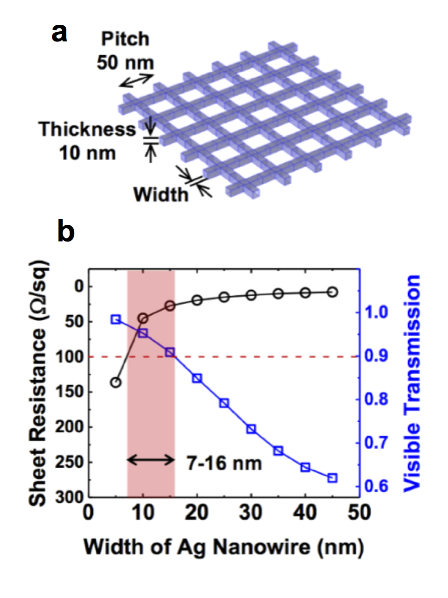
Based on optical simulations and conductivity calculations, we have devised design guidelines for metal nanowire meshes to maximize their conductivity and transmissivity (see Figure 5). We found that the ordered nature of the nanowires significantly decreases the average nanowire length required to maintain high conductivity, increasing defect tolerance. Furthermore, we evaluated and extracted relationships for how introducing anisotropy by changing nanowires’ periodicity or resistivity affects both electrical and optical performance. These design guidelines can help guide future fabrication and experimental studies.
Impact on Mission
This project is directly relevant to the Laboratory’s focus on advanced materials and manufacturing techniques for optical and energy applications. We have demonstrated a new fabrication technique to make subwavelength structures needed for optical metamaterials at visible wavelengths with tunable properties, and for transparent electrodes used in solar cells, photodetectors, and electronic displays. We have also developed computational tools for evaluating and guiding the development of these materials for their target applications.
The project also helped recruit a number of students and recent university graduates to the Laboratory, including a postdoctoral candidate who also gained project-management experience as the principal investigator of the project; two post-collegiate appointees, one of whom converted to a staff position; three summer undergraduate students; and one graduate student.
Conclusion
Our method of fabricating these fishnet metamaterials and transparent electrode nanowire meshes represents a fundamentally new approach that has attracted significant interest from both academic partners and large industrial firms (who were primarily interested in the transparent electrode applications) when we presented these preliminary results at the 2017 Materials Research Society Spring Meeting. We are currently exploring potential collaborations with both academia and industry to further evaluate and develop these materials.
References
Angelescu, D. E., et al. 2004. "Macroscopic Orientation of Block Copolymer Cylinders in Single-Layer Films by Shearing." Advanced Materials 16:1736–1740. doi: 10.1002/adma.200400643.
Bai, W., and C. A. Ross. 2016. "Functional Nanostructured Materials Based on Self-Assembly of Block Copolymers." MRS Bulletin 41(2):100–107. doi: 10.1557/mrs.2016.1.
Chai, J., et al. 2007. "Assembly of Aligned Linear Metallic Patterns on Silicon." Nature Nanotechnology 2(8):500–506. doi: 10.1038/nnano.2007.227.
Ellmer, K. 2012. "Past Achievements and Future Challenges in the Development of Optically Transparent Electrodes." Nature Photonics 6:809–817. doi: 10.1038/nphoton.2012.282.
Garcia-Meca, C., et al. 2011. "Low-Loss Multilayered Metamaterial Exhibiting a Negative Index of Refraction at Visible Wavelengths." Physical Review Letters 106:067402. doi: 10.1103/PhysRevLett.106.067402.
Hecht, D. S., et al. 2011. "Emerging Transparent Electrodes Based on Thin Films of Carbon Nanotubes, Graphene, and Metallic Nanostructures." Advanced Materials 23(13):1482–1513. doi:10.1002/adma.201003188.
Hu, L., et al. 2011. "Metal Nanogrids, Nanowires, and Nanofibers for Transparent Electrodes." MRS Bulletin 36(10):760–765. doi: 10.1557/mrs.2011.234.
Kim, S. Y., et al. 2014. "Metal-Containing Block Copolymer Thin Films Yield Wire Grid Polarizers with High Aspect Ratio." Advanced Materials 26(5):791–795. doi: 10.1002/adma.201303452.
Lee, J.-Y., et al. 2008. "Solution-Processed Metal Nanowire Mesh Transparent Electrodes." Nano Letters 8(2):689–692. doi: 10.1021/nl073296g.
Schurig, D., et al. 2006. "Metamaterial Electromagnetic Cloak at Microwave Frequencies." Science 314(5801):977–980. doi: 10.1126/science.1133628.
Shalaev, V. M. 2007. "Optical Negative-Index Metamaterials." Nature Photonics 1(1):41–48.
Shingyouchi, K., and S. Konishi. 1990. "Gradient-Index Doped Silica Rod Lenses Produced by a Solgel Method." Applied Optics 29(28):4061–4063. doi: 10.1364/AO.29.004061.
Smith, D. R., et al. 2000. "Composite Medium with Simultaneously Negative Permeability and Permitivity." Physical Review Letters 84(18):4184–4187. doi: 10.1103/PhysRevLett.84.4184.
Soukoulis, C. M., and M. Wegener. 2011. "Past Achievements and Future Challenges in the Development of Three-Dimensional Photonic Metamaterials." Nature Photonics 5(9):523–530. doi: 10.1038/nphoton.2011.154.
Urness, A. C., et al. 2015. "Arbitrary GRIN Component Fabrication in Optically Driven Diffusive Photopolymers." Optics Express 23(1):264–273. doi: 10.1364/OE.23.000264.
Veselago, V. G. 1968. "The Electrodynamics of Substances with Simultaneously Negative Values of Epsilon and Mu." Soviet Physics Uspekhi 10(4):509–514. doi: 10.1070/PU1968v010n04ABEH003699.
Visconti, A. J., and J. L. Bentley. 2013. "Fabrication of Large-Diameter Radial Gradient-Index Lenses by Ion Exchange of Na+ for Li+ in Titania Silicate Glass." Optical Engineering 52(11):112103–112103. doi: 10.1117/1.OE.52.11.112103.
Publications and Presentations
Feigenbaum, E., and A. M. Hiszpanski. 2017. “Phase Accumulation Tracking Algorithm for Effective Index Retrieval of Fishnet Metamaterials and Other Resonant Guided Wave Networks.” Journal of Optics 19(7). doi: 10.1088/2040-8986/aa751b. LLNL-JRNL-703042.
Hiszpanski, A. M., et al. 2017. “Nanometer-Scale Metal Meshes Across Device-Relevant Areas for Transparent Electrodes and Optical Metamaterials.” Spring Materials Research Society (MRS) Meeting, Phoenix, AZ, April 17–21, 2017. LLNL-POST-729139.
Leon, J. J. D., et al. 2017. “Design Parameters for Subwavelength Transparent Conductive Nanolattices.” ACS Applied Materials & Interfaces 9:35360–35367. doi: 10.1021/acsami.7b08446. LLNL-JRNL-732399.
Hiszpanski, A. M., et al. 2017. “Fabrication of Metal Nanowire Meshes Over Large Areas by Shear-Alignment of Block Copolymers.” Patent Application, 2017. IL-13111 LLNLP165.


