Christopher Spadaccini (14-SI-004)
Abstract
Additive manufacturing is a breakthrough technology that is revolutionizing domestic and global manufacturing. It creates the potential to engineer materials possessing desired structural, thermal, electrical, chemical, and photonic properties in a single package. While many types of additive manufacturing tools are commercially available, ranging from simple desktop thermoplastic printers to state-of-the-art laser powder-bed metal systems, there are still significant limitations. Some of these limitations include the ability to create components with mixtures of materials ranging from polymers to ceramics, metals, and semiconductors. Additionally, commercial platforms do not have the resolution to access unique and powerful physics at the microscale and nanoscale. Our goal with this project was to develop and thoroughly understand new design methodologies and manufacturing techniques that will enable us to produce specific multifunctional materials with mission-relevant applications ranging from stockpile stewardship to global security to nuclear fusion ignition. To achieve this goal, we executed two closely linked thrusts: inventing and developing new additive manufacturing processes and designing and characterizing multifunctional materials.
Background and Research Objectives
Our primary objectives with this project were: (1) understand and advance current manufacturing capabilities and create new manufacturing processes that can mix disparate material classes and fabricate unique designs from relevant materials at relevant length scales, (2) develop the ability to design multifunctional materials with previously unachievable combinations of functionalities, and (3) create and characterize a multifunctional material.
We were successful in making progress toward all three objectives. This includes the development of four unique new additive manufacturing techniques: (1) direct metal writing, (2) diode-based additive manufacturing, (3) holographic lithography, and (4) parallel optical tweezers, as well as design methods for combining electromagnetic and structural properties. Finally, we fabricated several multifunctional materials, most notably a compressible three-dimensional supercapacitor electrode constructed from printed graphene aerogel.
Scientific Approach and Accomplishments
Direct Metal Writing
Most metal additive manufacturing approaches are based on powder-bed melting techniques such as laser selective melting or electron beam melting, which often yield uncontrolled microstructures with defects (e.g., pores or microcracks) and residual stresses. Here, we introduce a proof-of-concept prototype of a three-dimensional metal free-form fabrication process by direct writing of metallic alloys in the semisolid regime. This process is achieved through controlling the microstructure and the rheological behavior of semisolid alloy slurries that demonstrate a well-suited viscosity and shear thinning property to retain shape upon printing. The ability to control microstructure through this method yields a flexible manufacturing route to fabricating three-dimensional metal parts with full density and complex geometries.
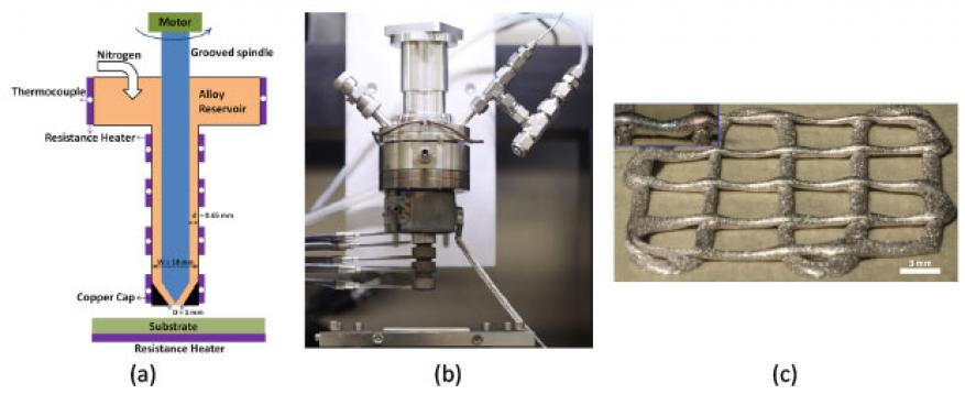
Based on a detailed study of the rheological properties, direct metal writing of the bismuth–tin compound Bi75Sn25 was carried out in the semisolid regime using a 1-mm-diameter nozzle robotically positioned by a three-axis motion stage, shown in Figure 1(a) and (b). The Bi75Sn25 metallic structures were printed onto a high-temperature masking-tape-covered steel substrate with an optional heater mounted on the underside. The nozzle-to-substrate distance was kept at approximately 0.7 mm to ensure moderate adhesion of the as-deposited filament to the substrate and between adjacent printed layers. As the metal slurry exits the nozzle, solidification rapidly occurs, which results in formation of a continuous filament retaining a rod-like shape.1 The marked shear thinning behavior and rapid solidification of the semisolid slurry collectively enable fabrication of three-dimensional overhanging structures where filaments can span over a wide unsupported region, as seen in Figure 1(c).
Diode-Based Additive Manufacturing
Selective laser melting of metal powder bed layers,2 whereby three-dimensional metal objects can be printed from a digital file with unprecedented design flexibility, is spurring manufacturing innovations in medical,3,4 automotive, aerospace,5 and textile industries. Because selective laser melting is based on raster-scanning a laser beam over each layer, the process is relatively slow compared to most traditional manufacturing methods (hours to days), thus limiting wide-spread use.
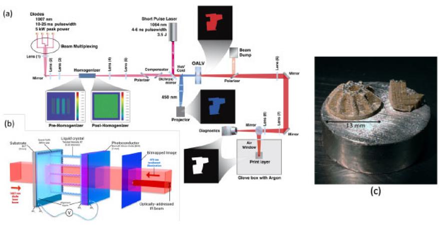
We have demonstrated an alternative method for creating additively manufactured metal parts using a wide area, optically addressable photomask supplied with a hybrid light source consisting of a low-cost diode laser array and a Q-switched laser (pulsed output beam). Because the majority of the heat input is supplied by the diode laser component, our system can be shown to scale more effectively as opposed to the more costly fiber-laser-based counterparts, even with the addition of the pulsed laser source. The novel use of an optically addressed light valve not only allows addressing on and off regions of the additive manufacturing process but also offers the ability to "gray scale" an image, providing selective thermal gradients to be imposed, and thereby potentially controlling residual stress and microstructure.6 Figure 2(a) and 2(b) show schematics of the system components and beam path. Figure 2(c) shows examples of sample parts fabricated with this prototype system in low-melting-temperature metals such as tin. Additionally, we have fabricated simple structures in high-temperature materials such as stainless steel to demonstrate a range of material options.
Holographic Lithography
As additive manufacturing technologies advance and mature, the geometric constraints imposed by fabricating two-dimensional planar layers become increasingly important to overcome. In the realm of light-driven additive manufacturing fabrication, holography provides a promising avenue toward true three-dimensional structures. Being capable of recording and reconstructing three-dimensional information, holographic shaping of the light field can enable direct three-dimensional fabrication in photopolymer resins. We have conceptualized, designed, and built a prototype holographic additive micro-manufacturing system, incorporating a liquid-crystal-on-silicon spatial light modulator to redirect light energy at the build volume by spatial control of the phase distribution.
Additive manufacturing processes with “volume-at-once” unit operations to produce complex three-dimensional structures in a single step have remained a major challenge. Some promising recent reports include the use of multi-beam interference to generate periodic three-dimensional lattice structures,7–10 and to modulate such lattices with aperiodic features.11–12 However, volume-at-once fabrication of aperiodic geometries that overcome the geometric limitations of these lattices has not previously been demonstrated.
The enabling technology is digital holography, a powerful paradigm for both recording and reconstructing three-dimensional geometrical information. Using a diffractive element to phase-modulate a coherent laser beam, multiple sub-images of a holographically shaped light field are directed such that they intersect within the resin volume. The light distribution is designed to deliver energy maxima to the desired regions of the resin that are to be cured. The part forms in situ in about 10 seconds, without requiring any support structure, nor layer-by-layer curing. Our initial results produced millimeter-scale parts with approximately100-μm resolution. Figure 3 shows an example of one of our initial fabricated parts.13
Parallel Optical Tweezers
Optical tweezers were first reported in 1970,14 and have since become a powerful tool for manipulating microscale and nanometer-scale particles. In the past few decades, two primary approaches (i.e., the scanning optical tweezers and the holographic optical tweezers) have been pursued as a means of increasing the number of particles that can be handled simultaneously using optical tweezers. However, to turn this exquisite particle manipulation approach into a three-dimensional fabrication technique, improved speed and area are required.
We have created a new optical tweezers approach, called scanning holographic optical tweezers, which drastically increases the working area of holographic optical tweezers while maintaining tightly focused laser traps. A 12-fold increase in working area has been demonstrated. The scanning holographic optical tweezers approach achieves its utility by combining the large working area of the scanning optical tweezers method with the flexibility of the holographic optical tweezers for simultaneously moving differently structured optical traps in and out of the focal plane. We have also demonstrated a new heuristic control algorithm for combining the functionality of the two approaches to efficiently allocate the available laser power among a large number of traps. The proposed approach shows promise for substantially increasing the number of particles that can be handled simultaneously, which would enable optical tweezers additive-fabrication technologies to rapidly assemble microscopic-granular materials and structures in reasonable build times. Figure 4(a,b) shows the optical tweezer assembly concept, and Figure 4(c) is an image of multiple particles manipulated in space.15
Design for Multifunctionality
We have developed the initial ability to computationally design for multiple functionalities with disparate physics. As an example, we demonstrated the design of a structural two-dimensional photonic crystal that combines Maxwell’s equations with structural mechanics. Photonic crystals are dielectric materials with a repeating unit cell structure. By correctly positioning dielectric material along with void space within the repeating unit cell, the photonic crystal can be designed to transmit or block electromagnetic waves at particular frequencies. Waves with frequencies that are blocked—those within the photonic band gap—are perfectly reflected, allowing the design of mirrors, internal waveguides, and resonant cavities for those frequencies. Wider band gaps are often desirable because they allow for mirrors, for example, which work over larger frequency ranges.
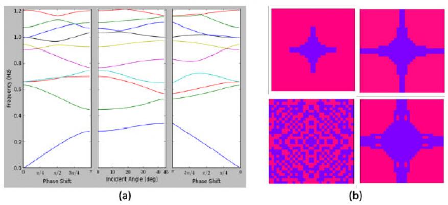
Many such photonic crystal designs exist in the literature. However, the optimal design for such materials are nonstructural, in the sense that the dielectric material forms discrete islands of various shapes and patterns surrounded by void space. Thus, the photonic crystals are not self-supporting, limiting their applicability. To address this design challenge, we created a two-dimensional optimization code that simulates both the electromagnetic and mechanical response of photonic crystals. We then sought to design the unit cells for crystals that exhibit the largest possible photonic bandgaps, subject to a lower bound on their stiffness. By keeping this lower bound well above zero, we can ensure that the materials are self-supporting. Figure 5 shows the band gap for one of our designs and some of the actual two-dimensional structures.
The two-dimensional code serves as a template for a three-dimensional code that will be developed later. Owing to the significantly increased computational cost of simulating the multiple physics in three dimensions, the follow-on code will be massively parallel, but the optimization problem itself remains essentially unchanged.
Impact on Mission
This project supported Lawrence Livermore missions in national security and energy security by developing techniques for manufacturing materials with applications in stockpile stewardship, materials and structures for defense uses, and materials and fabrication for high-energy-density laser targets. Our research directly aligns with LLNL's core competency in advanced materials and manufacturing. Several of the manufacturing techniques we developed will be of interest to Livermore programmatic application areas because of their ability to fabricate high-quality materials at relevant length scales. Additionally, some of the work in multifunctional design has led to a new design and optimization center within the Engineering Directorate at Livermore, as well as a significant Defense Advanced Research Project Agency program. Additionally, a new commercial partner Autodesk, a major design software firm, has partnered with Livermore for future work in this area. Finally, this work has resulted in significant high-impact publications including Nature Materials, Nature Communications, and Nano Letters. In the last year, our research has resulted in five journal covers. Finally, the intellectual property associated with our work is wide-ranging, with several dozen invention disclosures and many patent filings. In addition, we have recruited 25 students and 10 postdoctoral researchers to participate in this research effort.
Conclusion
We have developed four new additive fabrication techniques and enabled a new design and optimization effort at Lawrence Livermore. Much of this work will continue via programmatic applications, external research funding, or industrial collaborations. We have received two licensees for our diode-based additive manufacturing technology, a new Defense Advanced Research Project Agency program, a new design and optimization activity, and Livermore programmatic work for the National Ignition Facility and Weapons Complex Integration program, to name a few.
References
- Chen, W., et al., “Direct metal writing: Controlling the rheology through microstructure.” Appl. Phys. Lett. (in press).
- Kruth, J. P., et al., "Selective laser melting of iron-based powder." J. Mater. Process. Tech. 149, 616 (2004).
- Kruth, J. P., et al., Digital manufacturing of biocompatible metal frameworks for complex dental prostheses by means of SLS/SLM. Taylor & Francis Ltd., London, United Kingdom (2005).
- Vandenbroucke, B., and J. P. Kruth, "Selective laser melting of biocompatible metals for rapid manufacturing of medical parts." Rapid Prototyp. J. 13, 196 (2007).
- Vayre, B., F. Vignat, and F. Villeneuve, "Metallic additive manufacturing: state-of-the-art review and prospects." Mech. Ind. 13, 89 (2012).
- Matthews, M. J., et al., Diode-based additive manufacturing of metals. (2017).
- Xu, J., Fabrication of photonic quasicrystals using holographic lithography method. Hong Kong University of Science and Technology, Hong Kong, China (2007).
- Schaedler, T. A., et al., “Ultralight metallic microlattices.” Science 334(6058), 962 (2011).
- Ohlinger, K., et al., “Spatially addressable design of gradient index structures through spatial light modulator based holographic lithography.” J. Appl. Phys. 114(21), 213102 (2013).
- Ning, H., et al., “Holographic patterning of high-performance on-chip 3D lithium-ion microbatteries.” Proc. Natl. Acad. Sci. 112(21), 6573 (2015).
- Leibovici, M. C., G. M. Burrow, and T. K. Gaylord, “Pattern-integrated interference lithography: Prospects for nano-and microelectronics.” Optic. Exp. 20(21), 23643 (2012).
- Leibovici, M. C. R., and T. K. Gaylord, “Custom-modified three-dimensional periodic microstructures by pattern-integrated interference lithography,” J. Opt. Soc. Am. A, 31(7), 1515 (2014).
- Shusteff, M., et al., Additive fabrication of 3D structures by holographic lithography. 2016 Ann. Intl. Solid Freeform Fabrication Symp., Austin, TX, Aug. 8–10, 2016.
- Ashkin, A., “Acceleration and trapping of particles by radiation pressure.” Phys. Rev. Lett. 24, 156 (1970).
- Shaw, L. A., C. M. Spadaccini, and J. B. Hopkins, Scanning holographic optical tweezers. (2017).
Publications and Presentations
- Maiti, A., et al., “3D printed cellular solid outperforms traditional stochastic foam in long-term mechanical response.” Sci. Rep. 6 (2016). http://dx.doi.org/10.1038/srep24871
- Pascall, A. J., et al., “Light directed electrophoretic deposition for additive manufacturing: Spatially localized deposition control with photoconductive counter electrodes.” Key Eng. Mater. 654, 261 (2015). LLNL-JRNL-662724.
- Shaw, L. A., et al., “Holographic optical assembly and photopolymerized joining of planar microspheres.” Optic. Lett. 41, 3571 (2016). http://dx.doi.org/10.1364/OL.41.003571
- Shusteff, M., et al., Additive fabrication of 3D structures by holographic lithography. 2016 Ann. Intl. Solid Freeform Fabrication Symp., Austin, TX, Aug. 8–10, 2016. LLNL-CONF-697811.
- Shusteff, M., et al., 2016. Optimal source beam shaping for digital holographic lithography. 2016 Imaging and Applied Optics Congress, Heidelberg, Germany, July 25–28, 2016. LLNL-PROC-686328.
- Sullivan, K. T., et al.,"Controlling material reactivity using architecture." Adv. Mat. 28(10), 1934 (2015). LLNL-JRNL-654040. http://dx.doi.org/10.1002/adma.201504286
- Sullivan, K. T., et al., "Quantifying dynamic processes in reactive materials: An extended burn tube test." Propell. Explos. Pyrotech. 40(3), 394 (2015). LLNL-JRNL-663731.
- Zheng, X., et al., “Lightweight micro lattices with nanoscale features fabricated from projection microstereolithography.” 2014 IEEE 27th Intl. Conf. Micro Electro Mechanical Systems (MEMS), p. 510. Institute of Electrical and Electronics Engineers, Piscataway, NJ (2014). LLNL-CONF-646856.
- Zhu, C., et al., “Highly compressible 3D periodic graphene aerogel microlattices.” Nat. Comm. 6(6962) (2015). LLNL-JRNL-665510. http://dx.doi.org/10.1038/ncomms7962


