Lars Voss (16-FS-038)
Abstract
The aim of this work was to demonstrate the feasibility of using halogens such as chlorine, bromine, and iodine to depress the melting point of selenium to at or near room temperature while maintaining the semiconducting properties of liquid selenium. In particular, the use of Iodine-2 (I2) in a 50:50 atomic ratio with selenium (Se) was shown to result in a liquid semiconductor at < 60oC. Optical and electrical data confirmed that the band gap of the resulting material is 1.74 eV with a doping concentration in the range 1012—1013 cm−3. In addition, photo-current measurements on gold/selenium—iodine/gold structures and photopower measurements on n-gallium nitride/selenium—iodine/indium tin oxide devices confirm that the liquid mixture is suitable for use in a wide range of devices including radioisotope batteries, sensors, and electronics for harsh environments.
Background and Research Objectives
Typical semiconductors are solid materials, usually with a crystalline lattice but with important exceptions that are amorphous. A number of liquid semiconductors are known, including tellurium, selenium, and many binary chalcogenides such as lead (II) selenide, silver selenide, and zinc telluride.1 Of these, selenium is unique in that it has both the lowest melting point (220oC) and that it is elemental (except for the case of tellurium). Liquid selenium is also orders of magnitude less conductive than other liquid semiconductors, with a conductivity of ~10−8 Ω−1cm−1, a useful characteristic for many electronic devices as it indicates a low background carrier density and potentially long depletion width.1 Finally, many of the properties are agreeable including a reasonable band gap (1.8 eV), low hole concentration (3 × 1013 cm−3), and low but not unacceptable mobility (2 cm2/V-s).2
Nevertheless, the fact that the melting point is >200oC is a significant drawback that can add fabrication, packaging, and use complexity. A liquid semiconductor capable of operating at room temperature with reasonable electronic properties might find use in a number of applications, including radioisotope batteries,2–4 thermoelectrics,5 sensors for harsh environments (high temperature, high radioactive fields), direct ink writing of semiconductors, spin on semiconductors for low-cost large-area devices, large-volume devices, and new frontiers in liquid state physics. The reasons for this include the fact that with no crystal lattice, there is no need to achieve large, single crystals with low defect densities. A solution in the form of selenium/halide mixtures, in which the selenium is at equilibrium with a selenous halide (e.g., in the case of chlorine, a selenium/selemium (I) chloride mixture) or with the halide itself (e.g., selenium/iodine, where no secondary phases are present in the phase diagram), could reduce the melting point between −50oC to 220oC, depending on the selenium:halide ratio.3 However, these mixtures have never been tested for their semiconducting properties. We propose to create a range of mixtures of selenium/chlorine and selenium/iodine in order to determine whether the liquid selenium mixtures retain their semiconducting characteristics through the use of photocurrent measurements.
Scientific Approach and Accomplishments
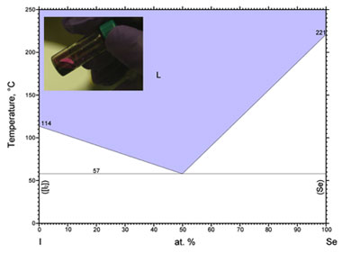
The focus of this work was the use of I2 mixed with selenium. I2 was chosen compared to chlorine gas and bromine gas for several reasons. Foremost is the fact that it does not form a compound with selenium, as chlorine gas (selenium (IV) chloride, selenium monochloride, selenium dichloride) and bromine gas (analogous compounds to chlorine gas) do. This is shown in the phase diagram in Figure 1, which depicts a continuous mixture of atomic iodine and selenium in equilibrium with each other and a eutectic (a mixture of substances in fixed proportions that melts and solidifies at a single temperature that is lower than the melting points of the separate constituents or of any other mixture of them) present at a 50:50 atomic ratio, which melts at 57oC.6
The method developed for preparing selenium:iodine mixtures was straightforward and performed in a nitrogen gas glove box. Calculated amounts of selenium and I2 were weighed on a balance and put into a sealed scintillation vial. All tests performed used approximately 50:50 atomic ratios of selenium:iodine. This was then placed on a hot plate set at 160oC, well above the melting point of pure I2. Relatively quickly, the I2 begins to melt and sublime. This is followed by selenium’s dissolving into the mixture (Figure 1 inset showing 50:50 liquid selenium:iodine mixture). After total dissolution of the selenium, the hot plate temperature was decreased to 60oC, just over the melting point of the eutectic (mixture of substances (in fixed proportions) that melts and solidifies at a single temperature that is lower than the melting points of the separate constituents). A micropipette was then used to transfer very small amounts (0.5—1 µL) of the liquid mixture onto the desired substrate, which was patterned with a polymer (SU-8) well to contain the mixture. A second substrate was then pressed on top of the droplet. This acted to spread the droplet so that it filled the well as well as seal the device by bonding with the SU-8. An additional sealant of ultraviolet-curable epoxy was then painted around the outside of the device and cured with a hand held ultraviolet light. It was observed that, properly prepared, the SU-8 and epoxy were fairly impervious to the Se:I mixture.
A variety of substrates were prepared in order to test various properties of the selenium:iodine mixture. The most successful were glass slides sandwich around the selenium:iodine for transmission measurements and n-gallium nitride and indium tin oxide for use in a sandwich structure to prepare a heterojunction diode for photopower measurements. This structure had previously been simulated using Silvaco, a finite element analysis semiconductor tool, to provide good performance as a power-generating device.
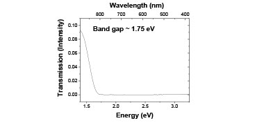
The first structure, glass slides sandwiching the selenium:iodine, was inserted into a J.A. Woollam alpha spectroscopic ellipsometer and the transmission was measured over the range 1.36—3.2 eV. Figure 2 shows the transmitted intensity of the light through approximately 20 µm of 50:50 selenium:iodine and 2 mm of glass at room temperature. Note the clear band edge observed, giving a band gap of approximately 1.7 eV. The transmitted intensity is fairly low due to the high thickness of the mixture.
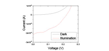
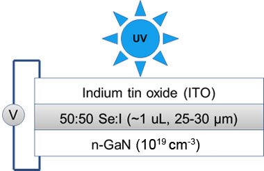
The n-gallium nitride/selenium-iodine/indium tin oxide structure is shown schematically in Figure 3 (SU-8 and epoxy encapsulant not shown). After fabrication, this device was measured as a function of temperature both in the dark and exposed to ultraviolet light from 24oC up to 80oC, in approximately 5oC steps. At 59oC, it was observed that the selenium:iodine had become a liquid, as predicted. At all temperatures, the structure behaved as a diode in the dark and as a photovoltaic cell when exposed to light. The IV curves showing such behavior as a liquid at 59oC are shown in Figure 4. The blue curve shows the dark current, which is very low around 0 V. Important parameters for liquid selenium reported in the literature or predicted by simulation compared with our measured values are shown in Table 1. Upon illumination, the short circuit current (Isc) at 0 V increases by 10,000x and an open circuit voltage (Voc) of 0.23 V is observed. Note that at room temperature the Voc was observed to be higher (0.42 V). Finally, the band gap was extracted from the reverse bias leakage current versus 1/T, giving a value of 1.74 eV, in excellent agreement with both the reported value for liquid selenium (1.74 eV) and our transmission measurement of the band gap.
In addition to photocurrent measurements, capacitance-voltage measurements were performed at room temperature in order to extract carrier density. A plot of 1/C2 versus V gave a value of 3.6 × 1012 cm−3, which is comparable to that reported in the literature (1012 cm−3). Extrapolation of the carrier density at 59oC using an Arrhenius plot of dark current versus 1/T yields a carrier density in the liquid state of 3.6 × 1013 cm−3, very close to the reported 3.6 × 1013 cm−3 reported for pure liquid selenium. This indicates that the selenium in the mixture is likely dominating these properties.
Table 1. Predicted/reported for liquid selenium and measured values for 50:50 Se–I.
| Predicted value | Measured value | |
| Band gap | 1.74 eV | 1.74 eV |
| Carrier concentration | 1012 cm−3 (RT), 3.6 × 1013 cm−3 (liquid) |
3.6 × 1012 cm−3 (RT), 3.6 × 1013 cm−3 (liquid) |
| Open circuit voltage | 0.68 V | 0.42 V (RT), 0.23 (59oC) |
Impact on Mission
This project is in line with the core competency of advanced materials and manufacturing, as it will enable a new class of semiconductor materials with unique properties that can be manufactured in unique ways relative to other semiconductors.Conclusion
These results provide clear evidence for the feasibility of using halogens to suppress the melting point of selenium while maintaining its semiconducting properties. These results will be used to develop room-temperature, high-power-density, alphavoltaic radioisotope batteries. Further fundamental work on device lifetime, characterizing the band lineups, and charge transport properties will be crucial to maximizing the device design and power output.References
- Enderby, J. E., and A. C. Barnes, “Liquid semiconductors.” Rep. Prog. Phys. 53, 85 (1990).
- Tsang, F., et al., Nuclear voltaic cell, US Patent 20060251204 A1 (Feb. 16, 2006).
- Wacharasindhu, T., et al., “Radioisotope microbattery based on liquid semiconductor.” Appl. Phys. Lett. 95, 014103 (2009).
- Wacharasindhu, T., et al., “Encapsulated radioisotope for efficiency improvement of nuclear microbattery.” Proc. PowerMEMS, Transducer Research Foundation, San Diego, CA, p.193 (2009).
- Wacharasindhu, T., and J. Wan Kwon, “Liquid semiconductor diode as a thermal harvester for high temperature applications.” Proc. PowerMEMS+microEMS, Transducer Research Foundation, San Diego, CA, p. 53 (2008).
- Okamoto, H., “I–Se (iodine–selenium),” Binary alloy phase diagrams. ASM International, Materials Park, OH (1990).


