Joshua Kuntz (15-ERD-043)
Project Description
We are extending the range of material transparency from optical towards microwave regimes by developing microscopic- and nanometer-scale structures that allow us to control and manipulate the electromagnetic response of materials. Such materials could have applications in a broad range of areas such as sensors, communications, solar cells, and lasers. It has been theoretically and empirically shown that arrays of these structures on and within materials can yield unique responses, such as eliminating optical reflection and increasing adhesive properties. We will utilize and develop modeling, synthesis, and fabrication techniques to design and implement complex structures with designed responses. Our primary goal is to use three-dimensional metamaterials—artificial materials engineered to have specific properties not usually found in natural materials—to extend the wavelength of absorbing materials such that a single material will be able to absorb several wavelengths from the visible towards the microwave regime.
To implement microscopic and nanometer-scale structured arrays onto surfaces for prescribed responses, we will institute a combined effort of modeling, fabrication, and characterization. By varying the process order of coating and etching for producing hierarchically structured composite materials, we hope to generate the widest possible range of hierarchies and thus produce wide-band metamaterials. We expect to design and fabricate optically transparent materials based on "meta-atoms" designed from polymers, dielectrics, metals, and semiconductors. A lattice of these meta-atoms will have a specific broadband transparency ranging from optical to possibly microwave regimes. We will work to extend the transparency range towards the microwave regimes by iterating with fabrication and then using electromagnetic simulation. Throughout, we will measure and characterize the reflectivity of each generation of material. With the final material, we will characterize the optical-to-microwave response by simulations under a variety of conditions, including extreme temperatures.
Mission Relevance
Broadband metamaterials have applications in a range of DOE and LLNL mission areas such as the use of sensors or lasers for applications in national and energy security. This initiative will leverage the investments made towards additive manufacturing while creating new materials with optimized physical properties, other than mechanical. Our project thus aligns well with LLNL's strategic plan, specifically the core competency in advanced materials and manufacturing.
FY16 Accomplishments and Results
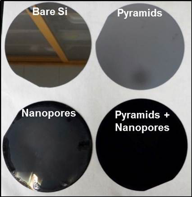
In FY16 we (1) produced broadband optical and infrared structures with controlled heirarchical structures with features in the micrometer- and nanometer-length scales (see figure), (2) determined that these structures possess superior electromagnetic properties over wider wavelength regimes than either feature independently; (3) determined that the measured performance of these hierarchical structures, less than 1% reflection from 250 to 2,500 nm, match the predicted performance modeled in FY15; (4) measured the inherent electromagnetic properties of our nanometer-scale composite carbon-loaded materials and, using this data, designed and modeled the performance of hierarchical radio-frequency structures, with controlled frequency response from 5 to 20 GHz; and (5) produced designs for model validation.


