Selim Elhadj (15-ERD-057)
Abstract
In this project, we assessed the lifetime laser-damage performance of semiconductor-based transparent-electrode materials by comparing the performance of conventional oxide materials with those of next-generation semiconductors. As a result, the highest lifetime damage performance of transparent-electrode materials was demonstrated, along with the fundamental insight that single-crystal systems are ideal materials for high-power optoelectronics applications. Polycrystalline systems, including oxide materials such as indium tin oxide, were limited by charge transport across grain boundaries, requiring high levels of free-charge carrier in the conduction band to reduce the energy barrier for transport. Free-carrier absorption then dominated the laser damage for such polycrystalline systems, while in single-crystal-semiconductor-based transparent electrodes localized defect-driven damage dominated (but at much higher laser damage thresholds). An atomistic view of the grain-boundary structures at the nanoscale was described by advanced molecular dynamics simulations that were experimentally validated, yielding fundamental insights into the quantized nature of nanoscale grain boundary states. Implementation of the materials that we assessed for optoelectronics devices can help push the performance limits of high-repetition-rate, high-power, high-energy laser systems.
Background and Research Objectives
Within an optical train, films and their interfaces are generally the weakest optically and they limit performance in high-power laser applications. Transparent electrodes (TEs) are especially problematic because free-charge carrier absorption makes them the failure point within optoelectronic devices crucial to laser systems for beam modulation and amplification. TEs must fulfill two conflicting functions. First, they must be electrically conductive for device actuation on length scales (up to tenths of a centimeter) and time scales (down to nanosecond rise times) that are compatible with the processing of large beam sizes. This requires a sheet resistance (Rs) of approximately 100 ohms per square (Ω/sq) or less. Second, they must transmit light with minimal absorption to avoid laser-induced heating. This is a requirement that is difficult to meet because, depending on the wavelength, the electrons in the conduction band will interact with light and absorb laser light energy that is converted to heat. In high-energy lasers (such as that used at Lawrence Livermore National Laboratory's National Ignition Facility), the high-energy pulses at near-infrared wavelengths (approximately 10 j/cm2 at 1,064 nm) could only be accommodated by using in-house plasma-gas electrode technology (Goldhar and Henesian 1984). However, plasma-gas electrodes cannot be switched fast enough for high-energy/high-repetition-rate laser systems used to achieve pulsed shots at tens or hundreds of hertz or higher. Solid films composed of indium tin oxide (ITO) and other oxides (such as n-doped zinc oxide) are the reference TE-material systems that can achieve both high transmission and conduction but are limited in their lifetime damage performance. Therefore, new TE materials and implementations are sought to develop TEs that can support development of next-generation high-average-power and high-energy laser systems.
Scientific Approach and Accomplishments
TEs are usually deposited as thin polycrystalline films. However, because nanoscale grain boundaries trap states impede charge transport, high levels of doping and free-electron densities greater than 1020 cm3 are required to overcome the energy barrier for charge transport in polycrystalline materials (Tsurumi et al. 1999). Therefore, using single-crystal film that is thermally robust with low doping and free-carrier density (but is also scalable to a large area) is ideal to produce TEs with higher resistance to damage. Both types of material systems were studied during this project.
We addressed the problem of lifetime laser damage to TEs by investigating the mechanism involved in laser-induced damage of TEs. We employed a heat-diffusion model and a critical temperature as the damage criteria. We also compiled a statistical description of defect distribution in the films. Based on the knowledge gained, our strategy to improve laser-damage performance included reduction of the laser energy absorption, increased heat dissipation, and selection of appropriate materials.
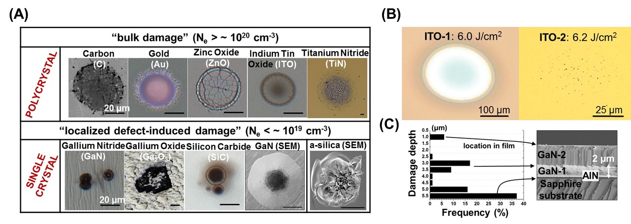
We addressed the problem of laser absorption by reducing free-carrier and defect absorption while increasing heat dissipation. This was achieved by using good thermal conductors and adding a capping layer as an additional mechanism for heat dissipation. Finally, we explored the use of third-generation [silicon carbide (SiC) and gallium nitride (GaN)] and fourth-generation [gallium(III) oxide (Ga2O3)] semiconductors commercially available as large-area, single-crystal films on substrates (Figure 1). All of the other film materials we investigated were deposited in-house using electron-beam deposition. The ITO films were deposited in a radio-frequency magnetron-sputtering-deposition system assembled specifically for this project. Figure 1 depicts two laser-damage morphologies related to the free-carrier density of neon (Ne) in single-crystal and polycrystalline widegap-semiconductor thin films. The polycrystalline films (composed of ITO, carbon, zinc oxide, and compounds) all appear to have been damaged by a bulk free-carrier absorption (Ne > 1020 cm3) process that ablates or cracks the film deterministically (i.e., the damage tracks the shape of the beam). In contrast, the single-crystal films (composed of GaN, Ga2O3, and SiC with Ne > 1019 cm3) all appear to have been damaged by defect-driven localized absorption events that manifest as small distributed pit-eruption events [Figure 1(A)] (Yoo et al. 2016). In other words, the bulk or “large damage” is eliminated as the dominant form of damage near the damage threshold of the material. At higher fluences, eventually the free-carrier driven and the defect-driven bulk damage occur simultaneously. Still, the threshold is increased in lower Ne materials.Thicker ITO films synthesized with high charge mobility and lower Ne (but still conductive within specification) were far less affected by laser damage. However, they exhibited morphologies characteristic of small defect-driven absorption mechanisms analogous to the single-crystal systems [shown in Figure 1(B)]. Most of the damage in single-crystal materials was initiated at interfaces of the film's layered structure [Figure 1(C)] from which high levels of defect-related photoluminescence were measured in GaN, SiC, and Ga2O3 films (data not shown).
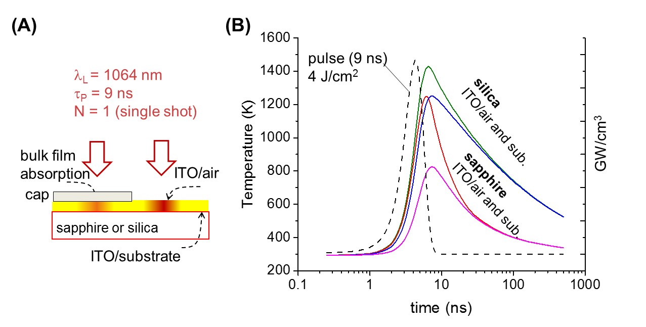
The pulsed-laser-induced bulk heating was captured by the simulated peak temperature in the ITO film based on the measured laser-absorption parameters and optical properties of the film at 1064-nm wavelength [Figure 2(A)].
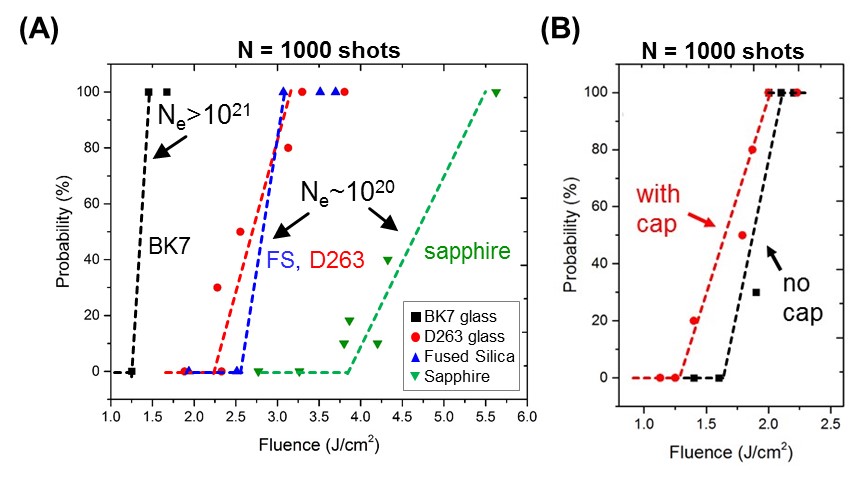
The temperature-time plot [Figure 2(B)] indicates that ITO film temperature should be significantly reduced with use of a substrate with high thermal conductivity, such as sapphire (as compared to silica glass) (Yoo et al. 2017). Likewise, the addition of a transparent alumina capping layer reduced the temperature rise compared to that of an uncapped ITO film (data not shown), suggesting that the use of sapphire substrate and a capping layer should improve damage performance. This approach was experimentally tested and the results are shown in Figure 3.
The lifetime damage performance can be determined using the fluency-dependent damage-probability curves for 1,000 pulse shots (Yoo et al. 2017). Figure 3(B) indicates that the lifetime performance of ITO was improved by a factor of approximately 2 over ITO on glass, and the ITO with a very high Ne (>1021 cm3) performed worse than those ITO films with lower Ne of approximately 1020 cm3. Surprisingly, although the single-shot (N = 1) performance was improved for the ITO with the cap layer (data not shown), the lifetime threshold with a cap layer was lower than without a cap [Figure 3(B)], likely due to new defects being introduced by the added cap layer (Yoo et al. 2017). In general, the ITO films that were made thicker (to maintain overall conductance and be less absorptive with lower Ne and higher mobility) exhibited improved lifetime performance (data not shown) (Yoo et al. 2017).
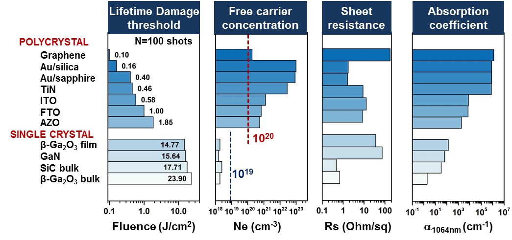
To identify good candidate TE materials, we assessed the lifetime damage performance of 11 materials, including metals, oxides, carbon, transition-metal nitride, and next-generation semiconductors with an Ne range spanning five orders of magnitude with Ne = 1018–1023 cm3 (Figure 4). The wide-gap, single-crystal, low-Ne materials exhibited laser-damage thresholds approximately 1 order of magnitude higher than that of the polycrystalline materials that generally required high levels of Ne for conduction to overcome GB barriers to transport. The lifetime threshold fluences >10 J/cm2 (1,064-nm wavelength) achieved are greater than current requirements for high-power, megajoule-class laser systems and near to the requirements of dielectric and bulk-crystal components currently in use in such lasers. The N = 100 shots are the number of exposures beyond which the thresholds remain fixed with N (data not shown). These threshold results demonstrate the highest damage performance for TEs, while still meeting baseline conduction and transmission values (data not shown) to be able to operate in high-repetition-rated optoelectronic devices used in large-aperture, high-power laser systems (see Figure 4).
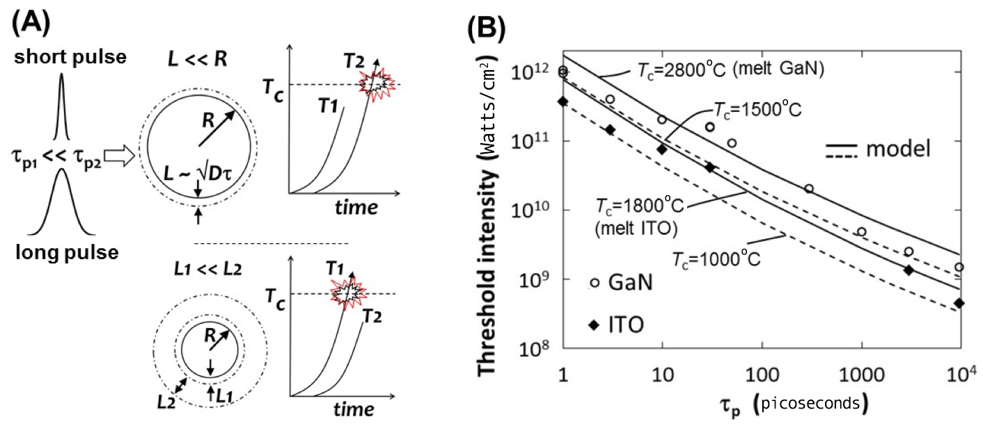
The damage behavior captured in the laser-damage test studies are rationalized by a heat diffusion model (see Figure 5), which can also describe the lifetime threshold versus N (data not shown). The basis of the model involves the use of a threshold damage criterion that corresponds to a specific heat-induced material transformation occurring at a critical temperature reached by an absorbing defect or material. For the model predictions, the thermal and optical properties of the absorbing material or defect were used and described reasonably well with the pulse-scaling data shown from picosecond to nanosecond pulse lengths [Figure 5 (B)]. The critical temperatures selected in the model to capture the damage onset ranged from the melting point of the materials down to the temperature rise related to the thermomechanical stress limit of the films (Elhadj et al. 2017, Yoo et al. 2016).
The dynamic structures of the GB defect states that control charge transport for lower Ne in polycrystalline systems were studied using high-resolution transmission electron microscopy with in situ heating measurements to validate molecular-dynamics simulations. The nanoscale GB dynamic mechanisms were then investigated using advanced computational simulation tools that revealed for the first time the quantized nature of the GB states that controlled grain growth and the final atomic GB structure on gold and copper model systems (Lange et al. 2016).
Impact on Mission
This work supports Lawrence Livermore National Laboratory's advanced materials and manufacturing core capabilities. The new computational capabilities we developed support NNSA goals of strengthening our science, technology, and engineering knowledge base. This research demonstrated new laser-damage performance-assessment capabilities based on next-generation semiconductor materials critical to the operation of future optoelectronic devices that can support amplification and aberration correction within high power laser systems. High-power lasers are also critical to scaling additive manufacturing processes. The fundamental molecular-dynamic simulations of nanoscale GBs were experimentally validated, providing new analytical methods for understating the microstructural behavior of materials subjected to heating or stress.
Conclusion
We explored new designs for large-area, high-power spatial-light modulators. The new spatial-light modulator designs can be implemented in the energy sections of the front end or back end of high-power laser systems for aberration corrections in turbulent environments or when heat is producing distortions in the amplification stage. They can also be used in next-generation additive-manufacturing-related beam-shaping technology. Developing high-power-handling optoelectronic materials such as the TE in this project can help to improve the performance levels of high-power laser systems.
References
Goldhar, J. and M. A. Henesian. 1984. "Electro-Optical Switches with Plasma Electrodes." Optics Letters 9 (3): 73–75. doi:10.1364/ol.9.000073.
Lange, A., et al. Forthcoming. "Kinetic Pathways of Metal Nanoparticle Coalescence." Acta Materialia.
Tsurumi, T., et al. 1999. "Electric Properties of Zinc Oxide Epitaxial Films Grown by Ion-Beam Sputtering with Oxygen-Radical Irradiation." Japanese Journal of Applied Physics 38, Part 1(6A): 3682–688. doi:10.1143/jjap.38.3682.
Yoo, J. H., et al. 2016. "Laser Damage Mechanisms in Conductive Widegap Semiconductor Films." Optics Express 24(16): 17616–634. doi:10.1364/oe.24.017616.
——— 2017. "Thermally Ruggedized ITO Transparent Electrode Films for High Power Optoelectronics." Optics Express 25(21): 25533–545. doi:10.1364/oe.25.025533.
Publications and Presentations
Elhadj, S. and J. H. Yoo. 2017. "Efficient Method for The Measurement of Lifetime Optical Damage Performance of Thin Film Coatings from Laser Damage Size Analysis." Optics Letters 42(16): 3153–156. doi:10.1364/Ol.42.003153. LLNL-JRNL-732604-DRAFT.
Elhadj, S., et al. 2017. "Optical Damage Performance of Conductive Widegap Semiconductors: Spatial, Temporal, and Lifetime Modeling." Optical Materials Express 7(1): 202–212. doi:10.1364/OME.7.000202. LLNL-JRNL-706843.
Elhadj, S. 2016. "High Optical Strength Widegap Conductive Semiconductors." SVC TECHCON 59th Annual Technical Conference, Indianapolis, IN, May 10–13, 2016. LLNL-PRES-692358.
——— 2017a. "Optical Damage of High-Performance Thin Film Transparent Electrodes (Keynote Presentation)." Laser-Induced Damage in Optical Materials 2017 (Thin Films), Boulder, CO, Sept 24–27, 2017. LLNL-PRES-738830.
——— 2017b. "Optical Damage Performance of Conductive Transparent Indiun Tin Oxide and Gallium Nitride: Spatial, Temporal, and Lifetime Modeling." 12th Pacific Rim Conference on Ceramic and Glass Technology, Honolulu, HI, May 21–26, 2017. LLNL-PRES-731415.
Lange, A. P., et al. 2016. "Dislocation Mediated Alignment During Metal Nanoparticle Coalescence." Acta Materialia 120: 364–378. doi:10.1016/j.actamat.2016.08.061. LLNL-JRNL-695366.
Yoo, J. H. 2016. "Laser Damage Mechanism of Wide Bandgap Conductive Semiconductors." SVC TECHCON 59th Annual Technical Conference, Indianapolis, IN, May 10–13, 2016. LLNL-PRES-691562.
Yoo, J. H., et al. 2016. "Laser Damage Mechanisms in Conductive Widegap Semiconductor Films." Optics Express 24 (16): 17616–634. doi:10.1364/Oe.24.017616. LLNL-JRNL-694293.
——— 2017a. "Thermally Ruggedized ITO Transparent Electrode Films for High Power Optoelectronics." Optics Express 25(21): 25533–545. doi:10.1364/oe.25.025533. LLNL-JRNL-737685.
——— 2017b. "Defect-Induced Optical Breakdown in Aluminum Nitride and Gallium Nitride Epitaxial Films." SPIE Optics and Photonics, San Diego, CA, Aug 28–Sept 1, 2016. LLNL-PRES-736585.


