Dongxia Qu (15-LW-018)
Abstract
Terahertz radiation falls in between infrared and microwave radiation in the electromagnetic spectrum. Like microwave radiation, terahertz radiation can penetrate a wide variety of nonconducting materials. The terahertz (THz) region, referred to as the wavelengths from 15 μm to 1 mm, remains one of the least-developed spectral regions, although proof-of-principle experiments have advanced its potential in a wide variety of application areas including homeland security, nondestructive evaluation, detection of explosives and noxious gases, medical imaging, material characterization, and broadband wireless communications. The three existing techniques for generation of broadband terahertz waves are: surface-field emission from semiconductors, photoconductive antennas, and optical rectification of ultrafast laser pulses. However, the bandwidth of terahertz emission generated by these techniques is typically limited to below 5 THz. The search for broader-band terahertz sources calls for new materials and mechanisms. Our objective was to develop a new mechanism of broadband terahertz radiation for national defense applications by taking advantage of the chiral spin texture of a new quantum state-of-matter topological insulator. A topological insulator is a material that behaves as an insulator in its interior, but whose surface contains conducting states, meaning that electrons can only move along the surface of the material. We used a photo-excited topological insulator heterostructure to generate a spin current, whose temporal evolution is dramatically faster than that of charge currents in conventional terahertz emitters. The resulting transient spin current can be converted into a broadband terahertz pulse via the inverse spin Hall effect. We demonstrated this spin–charge conversion mechanism in a proof-of-concept topological insulator with a gallium-arsenide heterostructure (a structure in which two semiconductor materials are grown into a "sandwich"). We discovered that the photo-induced spins can be driven from a topological insulator into an adjacent nonmagnetic semiconductor at room temperature. The interface spin transport leads to an inverse spin Hall photocurrent with a magnitude that is much larger and can be greatly modulated with an external electric field. The sensitivity of photocurrent to an external gate field, together with the observation of a distinct temperature-dependent photocurrent profile, allow us to isolate the interface spin transport solely arising from surface states, which were difficult to probe in microwave spin-pumping experiments. Our results provided the first experimental evidence to unambiguously isolate surface inverse-spin Hall current from the bulk contribution. In particular, we demonstrated the possibility to realize interface spin transport by seamlessly integrating a topological insulator thin film with a normal semiconductor. This possibility is of general interest in both fundamental physics and technological applications toward broadband terahertz generation and the emerging field of “topotronics,” in which quantum mechanical degrees of freedom are employed that allow for highly conducting dissipation-free channels at the surface of materials that would otherwise be insulating in their bulk.
Background and Research Objectives
One of the recent advances in spintronics is the development of nonmagnetic systems for a functional spintronic technology without the application of magnetic fields. The primary driving force of this research direction is the relativistic spin–orbit coupling that links an electron's momentum to its spin, and has led to a variety of new device paradigms, such as spin Hall effect transistors, spin–orbit torque memories, and broadband terahertz emitters.1–3 Topological insulators, a new class of quantum state of matter, is a promising material for spintronic applications owing to its exceptionally strong spin–orbit coupling.4 Considerable effort has been devoted to investigating the interaction of a topological insulator and a ferromagnetic material. However, ferromagnets might disrupt topological surface states near the Dirac point, leading us to explore the possible spintronic functionality and interface physics between a topological insulator and a nonmagnetic semiconductor.
We investigated the use of topological surface states to generate a net spin current, which could consequently flow into an adjacent semiconductor. The resulting spin current was then converted to a charge current via the inverse-spin Hall effect, leading to terahertz radiation. Our project focused on the demonstration of efficient spin excitation and spin injection from a topological insulator into a nonmagnetic semiconductor, and the detection of charge current in a topological insulator with a gallium-arsenide (GaAs) heterostructure. In this project, we (1) achieved proof-of-principle spin current injection and manipulation using a GaAs topological insulator heterostructure, (2) set up a terahertz time-domain spectroscopy system and conducted ultrafast terahertz spectroscopy experiments, (3) developed a near-infrared scanning photocurrent spectroscopy system, and (4) fabricated topological-insulator thin films on various substrates and obtained scanning photocurrent spectroscopy measurements. The progress we achieved in investigating the spin injection mechanism in topological insulator heterostrucures has provided the foundational work for the development of a photo-excited terahertz emitter.
Scientific Approach and Accomplishments
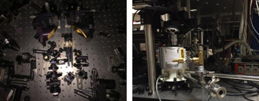
We first developed the terahertz-time-domain spectroscopy system as shown in Figure 1, which is a powerful tool to characterize the far-field temporal waveform of pulsed terahertz radiation from device surfaces. To demonstrate the interface spin injection mechanism, we further developed a low-temperature scanning photocurrent spectroscopy apparatus. This apparatus used a liquid-helium-cooled probe station in which a three-axis piezo-based nanometer-scale positioner was mounted on the cold finger in vacuum. The device was mounted onto the nanometer-scale positioner and obliquely illuminated with a thulium-fiber laser beam chopped at a frequency of 238 Hz.
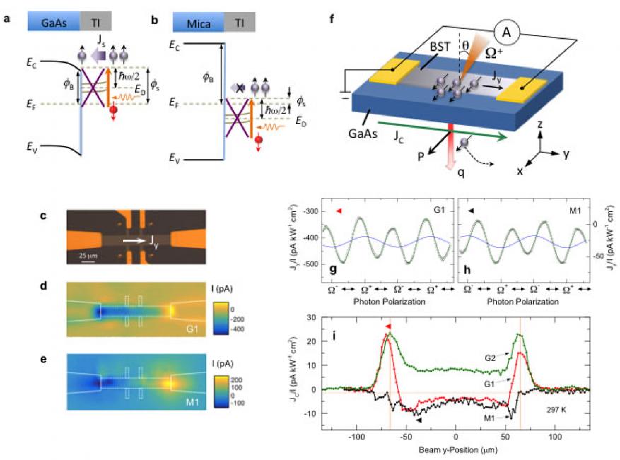
Figures 2(a) and 2(b) illustrate the proposed mechanism of gate-controllable spin transport at the interface of the topological insulator and the semi-insulating GaAs. When a circularly polarized light is incident on a topological insulator, spin-polarized electrons are excited from the surface valence band below the Dirac point to the conduction band with a hot electron energy φS. Because of spin-selection rules, such an interband transition generates a nonequilibrium surface spin accumulation. When φS is higher than the barrier height φB formed at the GaAs topological-insulator heterojunction, spin-polarized hot electrons could transport from the topological insulator into the GaAs and result in a perpendicular spin current, which is then transformed into a detectable charge current via the inverse-spin Hall effect of the topological insulator. When φS < φB—for example, in the topological-insulator/mica sample shown in Figure 2(b)—photo-excited carriers could not be injected into the substrate and no perpendicular spin current flowed.
Our experiments were performed on a series of samples consisting of 6 to 10 quintuple layers of (Bi0.5Sb0.5)2Te3 (bismuth antimony telluride, or BST), thin films grown on (111) semi-insulating GaAs and mica substrates by molecular beam epitaxy.5 The thin films are patterned into Hall bar structures 130-μm long and 20-μm wide, with electrical contacts made from 20-nm chromium/100-nm gold, as shown in Figure 2(c). We took the origin of our coordinate system to be the center of the channel. The 10-quintuple-layer BST/GaAs sample is p-type, whereas the 6-quintuple-layer BST/GaAs and 6-quintuple-layer BST/mica samples are n-type. Additionally, the BST/GaAs and BST/mica samples exhibited similar two-dimensional photocurrent profiles when the incident light is linearly polarized, as shown in Figures 2(d) and 2(e).
The polarization-dependent photocurrent response in the BST/GaAs and BST/mica samples displays opposite polarities near metal contacts. In Figures 2(e) and 2(f), we plot the raw traces of Jy versus photon polarization (black circles) in a 6-quintuple-layer BST/GaAs sample G1 and 6-quintuple-layer BST/mica sample M1, respectively. The data can be well fit to Jy(α) = C sin2α + L1 sin4α + L2 cos4α + D, where α is the angle between the polarization direction of incident light and the optical axis of the λ/4 waveplate, C is the amplitude of circular photocurrent JC that is helicity-dependent, L1 and L2 are the amplitudes of linear photocurrent that is helicity-independent and depends on the linear polarization of the light, and D is the amplitude of the polarization-independent photocurrent that primarily comes from the thermoelectric effect. Strikingly, the extracted circular-photocurrents JC are opposite in sign for two structures (blue curves), indicating they originate from distinct mechanisms. Indeed, the moving direction of JC in sample G1 near the electrode is consistent with predictions from the spin-diffusion process.
We next mapped out the one-dimensional spatial profile of JC along the y axis by repeating light polarization scans at each position in samples G1, M1, and p-type 10-quintuple-layer BST/GaAs sample G2 as shown in Figure 2(i). For sample G1, JC is negative at the center and rapidly changes sign when approaching the electrodes. The reverse of JC direction may be caused by the upward band-bending of the topological insulator near the electrode, which tunes the hot electron energy φS higher than the barrier energy φB, inducing the spin-diffusion current. For sample G2, JC is a maximum at the topological insulator–electrode interface and reaches a positive plateau at −50 mm < y < 50 mm, because φS is larger in p-type samples than in n-type samples, which leads to φS > φB in the middle of the p-type channel. By contrast, for sample M1, JC is negative and falls off quickly towards the electrode, in agreement with the previous observation of topological insulators on insulating substrates.
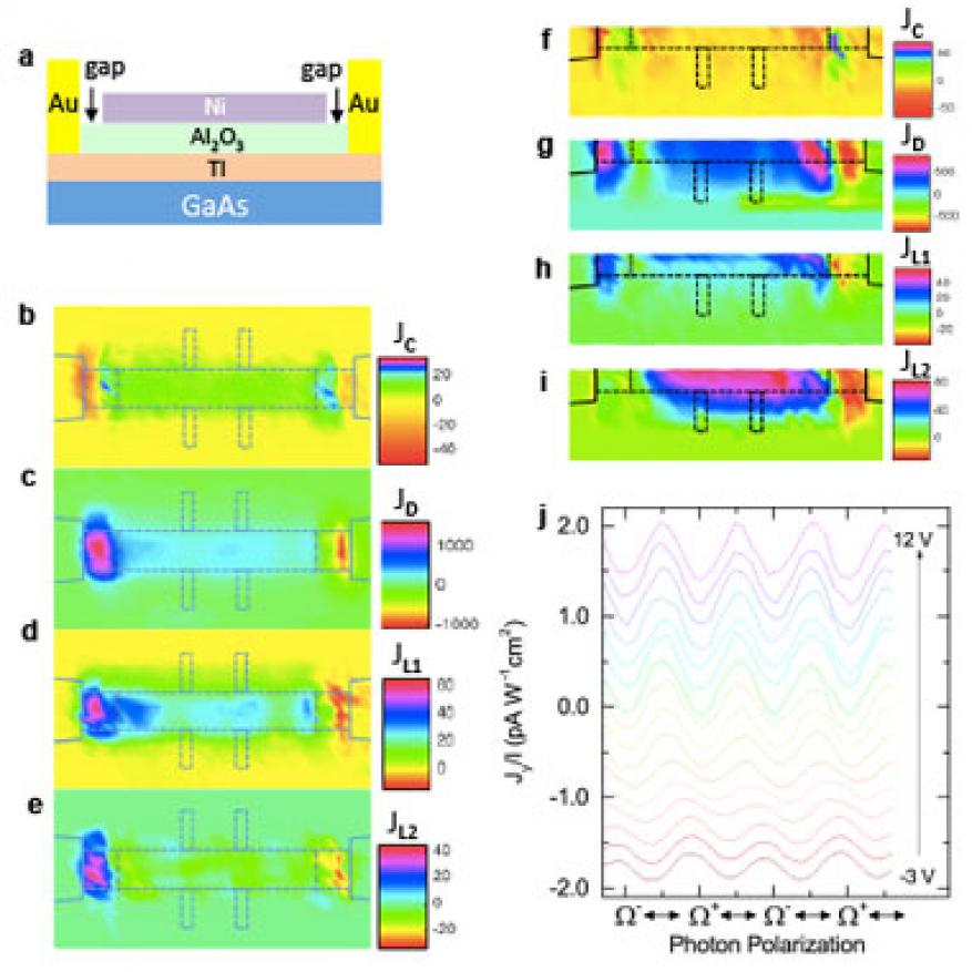
To further confirm the hypothesis of spin transport mechanism at the topological insulator/GaAs interface, we measured the dependence of the photocurrent on gate voltage VG, because gating may modulate hot electron energies above or below the energy barrier in a controllable manner. Our top-gate device was prepared by fabricating a semitransparent 10-nm nickel electrode on top of an aluminum-oxide insulated 8-quintuple-layer BST/GaAs sample, shown in Figure 3(a). In Figures 3(b) through 3(e), we map out the two-dimensional images of JC, JD, JL1, and JL2 in a top-gated sample at VG = 0 V and T = 25 K. The JC under the gate is uniform over a length of about 93 mm and increases near the contacts. Interestingly, the signal changes sign near the edges of electrodes, because the gap between the gate and the gold contacts induces a step-like laser intensity variation that drives hot electrons to move in a lateral direction rather than to inject into GaAs. As a result, the photogalvanic effect dominates in this region and JC reverses sign.
When VG = 8 V, the topological insulator/GaAs heterostructure exhibits a very different photocurrent behavior under the gate electrode. At T = 25 K, JC displays a positive signal, with a sign consistent with the photogalvanic effect in topological insulators on insulating substrates, as shown in Figure 3(f). In Figure 3(g–i), the JD and JL1 maps become less uniform, and JL2 displays a sign reversal compared to the value at VG = 0 V. Figure 3(j) shows the traces of Jy versus photon polarization at the center of the channel, while stepping VG from −3 to 12 V. The magnitude and extrema of Jy strongly depends on VG, and the polarity of JC can be completely switched as the external gate field is increased.
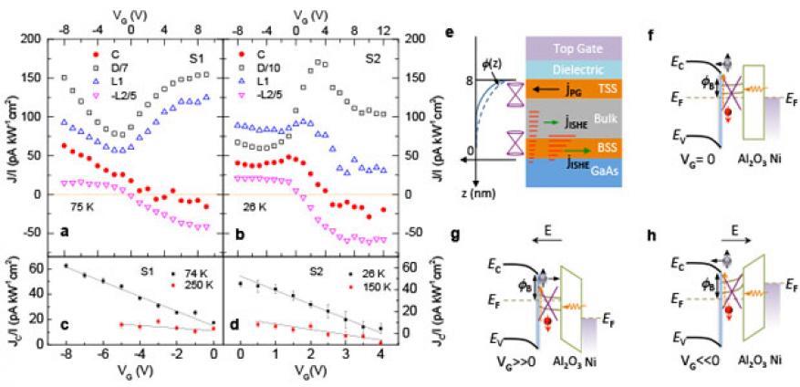
The extracted JC, JD, JL1, and JL2 versus gate voltage are summarized in Figure 4(a,b), measured on two samples S1 and S2, in which the applied gate voltage VG changes JC from negative to positive at VG0 = 2 and 4 V, respectively. The expanded view in Figure 4(c,d) reveals that JC linearly increases versus |VG − VG0| (VG < VG0), and the slopes decrease as temperature T is raised from 26 to 250 K.
We attribute the behavior of JC to the coexistence of interface spin transport and photogalvanic effect, as illustrated in the band diagrams under different gate voltages, as shown in Figure 4(e–h). Without photoexcitation, surface Dirac fermions do not move along the z direction because of their two-dimensional band nature. However, on the bottom surface, photo-excited electrons could transport into the substrate as a result of the absorption of extra kinetic energy from incident photons and subsequently generate a spin gradient within the penetration layer of surface states. When VG << 0, as shown in Figure 4(e), a negative VG induces a downward band-bending towards GaAs with φS > φB, which drives hot electrons across the topological insulator/GaAs interface to produce a perpendicular spin current. When VG ~ 0, there is little band-bending and the light penetration depth is 27 times larger than the sample thickness, resulting in a uniform photo-excited bulk electron density along the z axis. When VG >> 0, EF rises far above the Dirac point, resulting in φS < φB, which prevents hot electrons from moving towards GaAs. Therefore, at VG > VG0, the inverse spin-Hall-effect-induced photocurrent is negligible and a negative photogalvanic current dominates.
Impact on Mission
The development of novel terahertz sources is strongly tied to national defense issues including defense against explosives and noxious gases of mass destruction, real-time monitoring of terrorist activities, and actual battlefield imaging (e.g., enhanced identification and end-game missile guidance). Therefore, our research on creating wideband terahertz sources supports a central Laboratory mission in national security and the core competency of advanced materials and manufacturing. In addition, it is well aligned with the core competency in lasers and optical science and technology.
Conclusion
Our work demonstrates the use of a topological insulator/semiconductor interface to electrically tune the spin configuration of a photo-excited topological insulator. Manipulation of the interface spin accumulation was verified by detecting the helicity-dependent photocurrent within the topological insulator thin film. Electrically controllable spin properties of the topological insulator heterostructure may enable novel optoelectronic device applications—for example, a polarization-sensitive broadband photodetector in which the detection bandwidth is no longer restrained by photon energies above the band gap of the semiconductor, but determined instead by the photon energies above the barrier of hetero-junction. The interface spin transport revealed here may pave the way towards the room-temperature topological spintronic devices and inspire new device concepts that go beyond conventional materials and existing effects.
References
- Kato, Y. K., et al., “Observation of the spin Hall effect in semiconductors.” Science 306(5703), 1910 (2004). http://dx.doi.org/10.1126/science.1105514
- Wunderlich, J., et al., “Spin Hall effect transistor.” Science 330(6012), 1801 (2010). http://dx.doi.org/10.1126/science.1195816
- Kampfrath, T., et al., “Terahertz spin current pulses controlled by magnetic heterostructures.” Nat. Nanotech. 8, 256 (2013). http://dx.doi.org/10.1038/nnano.2013.43
- Qu, D.-X., et al., “Quantum oscillations and Hall anomaly of surface states in the topological insulator Bi2Te3." Science 329(5993), 821 (2010). http://dx.doi.org/10.1126/science.1189792
- He, L., et al., “Evidence of the two surface states of (Bi0.53Sb0.47)2Te3 films grown by van der Waals epitaxy.” Sci. Rep. 3, 3406 (2013). http://dx.doi.org/10.1038/srep03406
Publications and Presentations
- Qu, D.-X., et al., Spin manipulation at the interface of a topological insulator/GaAs heterostructure. American Physical Society March Mtg., Baltimore, MD, Mar. 14–18, 2016. LLNL-PRES-685697
- Qu, D.-X. et al., Circular photocurrent response of a topological insulator thin film probed by scanning photocurrent microscopy. American Physical Society March Mtg., San Antonio, TX, Mar. 6, 2015. LLNL-PRES-668068
- Qu, D.-X., Spin manipulation at the interface of a topological insulator/semiconductor heterostructure. (2016). LLNL-PRES-706806.
- Qu, D.-X., Topological insulators for next generation electronics and photonics. (2016). LLNL-PRES-670115.


