Christine Orme (16-ERD-033)
Executive Summary
We are developing an experimental and theoretical framework for the design of materials with a wide range of sizes from the molecular to micrometers that are composed of artificial-atom building blocks. This research into quantum dot superlattices and their various electronic and sensor applications supports the DOE goal of strengthening the connection between advances in fundamental science and innovation.
Project Description
Three-dimensional nanometer-scale crystal assemblies represent a new form of solid material that, if well coupled, can have properties derived from both their individual building blocks as well as emergent cooperative interactions. One of the stumbling blocks for developing these novel materials is the ability to control the crystalline quality of the assemblies using a fast and scalable process. Our work will develop an experimental and theoretical framework capable of describing and guiding the design of mesoscopic materials (between the size of a molecule and of materials measuring micrometers) composed of artificial-atom building blocks. To accomplish this, we will take advantage of LLNL's recent electrophoretic deposition additive-manufacturing technique, which is a novel approach to synthesizing three-dimensional nanocrystal assemblies that holds promise for a high degree of order, coupling, and device integration. Our first objective is to control the coupling order and device integration of superlattice arrays. The second objective focuses on the properties and cooperative phenomena that arise from assemblies of nanocrystals using both experimental and theoretical approaches.
We are motivated by the development of an emerging branch of materials science and materials physics based on coupled quantum-confined solids. This area is well developed and highly productive for two-dimensional nanometer-scale laminate structures, but has not been fully realized in three dimensions because of the difficulty in fabricating the materials. From a fundamental science perspective, it is predicted that coupled quantum dots (nanometer-scale crystals made of semiconductor materials that are small enough to exhibit quantum mechanical properties) can be used to generate novel materials with currently unrealized magnetic order, metal and insulator transitions, or electronic topological phase transitions. From a nanotechnology perspective, three-dimensional quantum dot superlattices have a broad range of applications in optoelectronics, magnetic storage, biosensors, and high-speed switching. The long-term vision for this capability is an ability to print materials in three dimensions with arbitrary band structures, including those that do not currently exist in the periodic table. We expect, if successful, to demonstrate control over ordering and patterning in three dimensions of single- and multiple-component materials. We intend to demonstrate new functions of materials from coupling of nanometer-scale crystals. We will also develop a model that describes new electronic and optical functionality. Finally, we will demonstrate an ability to design materials with specific properties.
Mission Relevance
By employing base materials and techniques developed within the Laboratory's manufacturing initiative and adding new functionality, we are supporting the core competency in advanced materials and manufacturing, employing techniques relevant to high-performance computing, simulation, and data science. Further, this research into quantum dot superlattices and their various electronic and sensor applications supports the DOE goal of strengthening the connection between advances in fundamental science and innovation. Our experimental and theoretical components are highly integrated, both informing each other and emblematic of the Laboratory's approach to research.
FY17 Accomplishments and Results
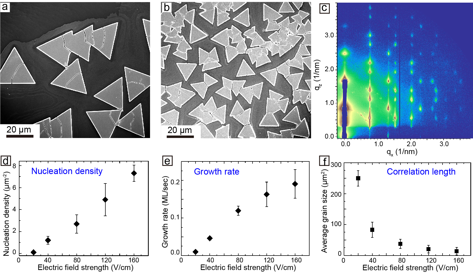
A central hypothesis for our project is that electric fields can drive growth of nanocrystal superlattices. To that end, in FY17 we (1) met our objective of demonstrating control over ordering and patterning of metallic nanoparticles as documented in a provisional patent (see figure); (2) developed an in situ growth cell and made the first x-ray scattering measurements demonstrating crystallization progression; and (3) found that some materials form thin films and appear to grow via a layer-by-layer mechanism, whereas others form facetted colloidal crystals and grow via a nucleation and growth model—this difference in behavior was unexpected, and we will explore various reasons for these differences in FY18. An understanding of these effects has taken priority over understanding pressure effects.
Publications and Presentations
Orme, C. 2017. "Reversible, Tunable, Electric-Field Driven Assembly of Silver Nanocrystal Superlattices." Nano Letters 17:3862–3869. doi: 10.1021/acs.nanolett.7b01323. LLNL-JRNL-710158.
Orme, C. A., et al. 2017. "Reversible, Field-Driven Superlattice Formation." LLNL-POST-740786.
Yu, Y., and C. Orme. 2017. "Electric Field-Driven Assembly of Silver Nanocrystal Superlattices." 2017 MRS Spring Meeting and Exhibit, Phoenix, AZ, 17–21 April 2017. LLNL-PRES-729482.


